IPC-SM-782A 表面安装设计和焊盘设计标准(带BGA).pdf - 第23页
solder joint dimension and the square root of the sum of the squares are added for outer land pattern dimensions and subtracted for inner land pattern dimensions. The result provides the final land pattern dimensions (Z, …

basic dimension of the spacing of one component lead ter-
mination or castellation to its adjacent counterpart(s). No
tolerance is assigned to pitch in the profile dimensioning
concept. Differences in pitch shall be included in the width
dimensions of the lead, termination, or castellation which
are dimensioned as basic at the minimum size.
3.3.2 Land Tolerancing
Profile tolerancing is used for
lands in a manner similar to that of the components. All
tolerances for lands are intended to provide a projected
land pattern with individual lands at maximum size. Uni-
lateral tolerances intend to reduce the land size and thus
result in a smaller area for solder joint formation. In order
to facilitate companion dimension systems the land pattern
is dimensioned across outer and inner extremities.
The dimensioning concept in this standard uses limiting
dimensions and geometric tolerancing to describe the
allowable maximum and minimum dimensions of the land
pattern. When lands are at their maximum size, the result
is a minimum acceptable space between conductors; con-
versely when lands are at their minimum size, the result is
the minimum acceptable land pattern necessary to achieve
reliable solder joints. These thresholds allow for gauging of
the land pattern for go/no-go conditions. The whole con-
cept of the dimensioning system described in this docu-
ment is based on these principles and extends to compo-
nent mounting dimensions, land pattern dimensions,
positioning dimensions etc., so that the requirements may
be examined using optical gauges at any time in the pro-
cess in order to insure compliance with the tolerance analy-
sis.
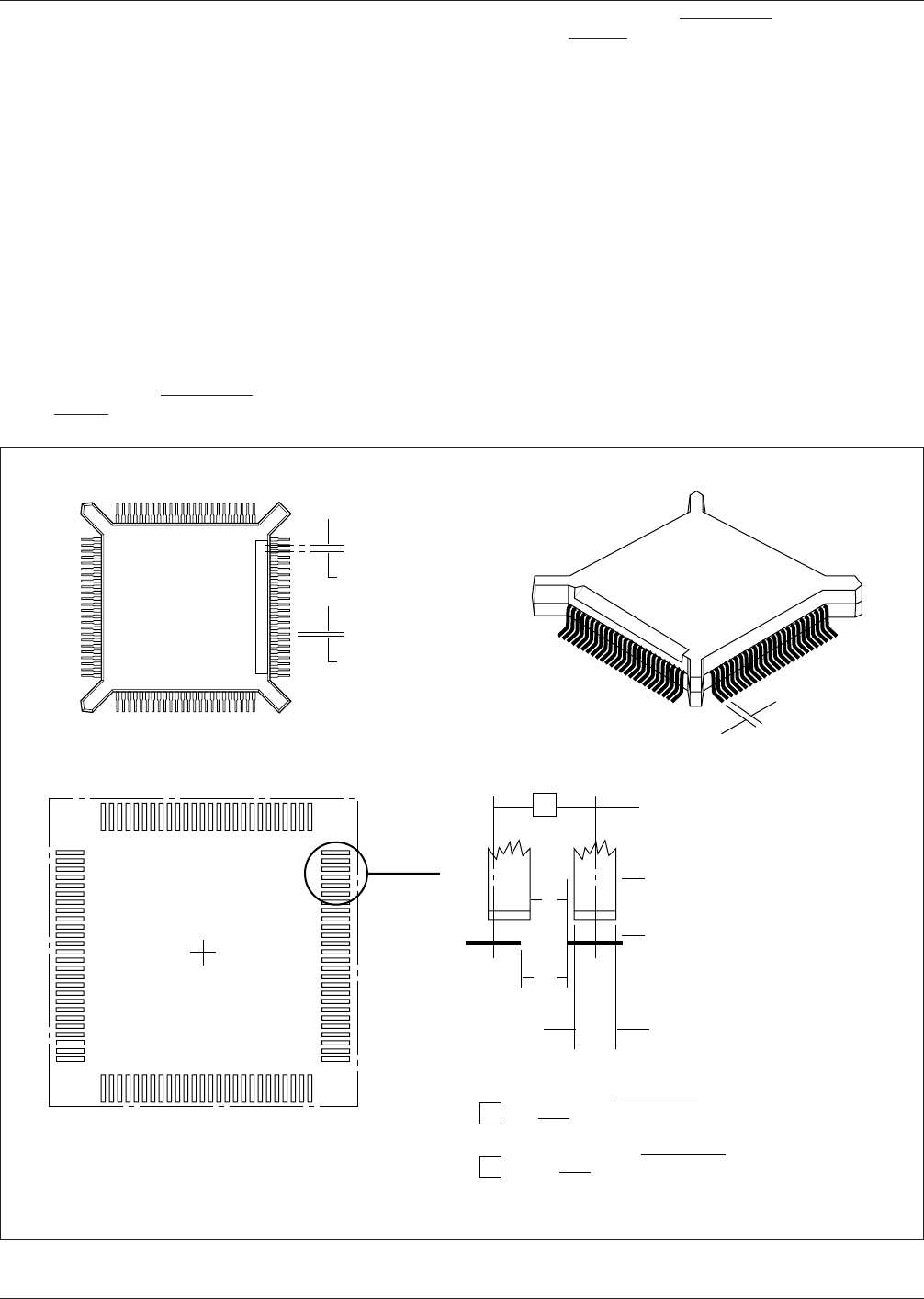
Figure 3–5 shows the land pattern for an SOIC with gull-
wing leads intended to be a companion to the chip compo-
nent dimensioning concepts shown in Figure 3–4. The
basic dimension is across the outer extremities.
Dimension ‘‘Z’’ is at maximum size, while the inner
extremities (dimension ‘‘G’’) are dimensioned at minimum
size. Unilateral tolerances decreased the basic dimension
for ‘‘Z’’ while increasing the basic ‘‘G’’ dimension. This
action results in a reduced land pattern, thus processing
target values should be as close to the basic ‘‘Z’’ and ‘‘G’’
dimensions as possible. This concept also holds true for the
width (X) of the land dimension which is specified at maxi-
mum size.
3.3.3 Dimension and Tolerance Analysis
In analyzing
the design of a component/land pattern system, several
things come into play. The size and position tolerances of
the component lead or termination, the tolerances of the
land pattern, the placement accuracy of the man/machine to
center the part to the land pattern, and finally the amount
of solder area available for a solder joint for formation of
a toe, heel or side fillet.
System equations have been developed for chip compo-
nents and multiple leaded parts. These concepts assume
that the target values of parts and land patterns are maxi-
mized to reflect solder joint formation (i.e., outer dimen-
sions of components at minimum size with outer dimen-
sions of land patterns at maximum size). The equations use
the following symbols:
C = the unilateral profile tolerance(s) for the component
F = The unilateral profile tolerance(s) for the board land
pattern
P = the diameter of true position placement accuracy to
the center of the land pattern
With the assumption that a particular solder joint or solder
volume is desired for every component, some methods use
the worst case criteria for determining a dimension. This
would require that ‘‘C,’’ ‘‘F,’’ & ‘‘P’’ be added to the mini-
mum dimension of the component length plus the solder
joint requirements, in order to determine the maximum
dimension of the outer land pattern.
Experience shows that the worst case analysis is not always
necessary, therefore statistical methods are used by taking
the square root of the sum of the squares of the tolerances.
This method assumes that all features will not reach their
worst case. The equations for determining chip component
land pattern requirements are as follows:
Z max = L min + 2J
T
+
√
C
L
2
+ F
2
+ P
2
G min = Smax–2J
H
–
√
C
S
2
+ F
2
+ P
2
X max = W min + 2J
S
+
√
C
W
2
+ F
2
+ P
2
Where:
Z = Overall length of land pattern
G = Distance between lands of the pattern
X = Width of land pattern
L = Overall length of component
S = Distance between component terminations
W = Width of component
J = Horizontal dimension of solder fillet
J
t
= Solder fillet at toe
J
h
= Solder fillet at heel
J
s
= Solder fillet at side
C = Component tolerances
C
L
= Tolerance on component length
C
S
= Tolerance on distance between component
terminations
C
W
= Tolerance on component width
F = Printed board fabrication (land pattern geometric)
tolerances
P = Part placement tolerance (placement equipment
accuracy)
The formula (the square root of the sum of the squares) is
identical for both toe and heel solder joint formation (dif-
ferent tolerances are used, however). However, the desired
IPC-SM-782A December 1999
14
电子技术应用 www.ChinaAET.com
solder joint dimension and the square root of the sum of the
squares are added for outer land pattern dimensions and
subtracted for inner land pattern dimensions. The result
provides the final land pattern dimensions (Z, G, and X) for
chips.
The same concept is true for multiple leaded or leadless
components. Additionally, pitch with land-to-lead overlap
(M) can be evaluated as well as the space (N) to reflect the
clearance between a lead, termination, or castellation and
the adjacent land(s). These latter values are not used in the
equations to determine the land pattern sizes, but may be
used to limit lead-to-adjacent land proximity and to adjust
lead-to-land overlap. See Figure 3–6.
The equation for determining if the clearance ‘‘N’’ or the
attachment overlap ‘‘M’’ are sufficient is as follows:
M =
[
W + X
2
]
−
√
C
2
+ F
2
+ P
2
N = E–
[
W + X
2
]
+
√
C
2
+ F
2
+ P
2
3.3.3.1 Tolerance Analysis
The following tolerance
concepts are used to determine the land patterns for all
electronic components. These concepts are detailed in
Table 3-4, and reflect the tolerances on the component, the
tolerances on the land pattern (on the interconnecting sub-
strate), and the accuracy of the equipment used for placing
components.
Solder joint minimums are shown for toe, heel and side fil-
lets. These conditions are minimum, since the equations in
3.3 address the tolerance of component, board, and place-
ment accuracy tolerances (sum of the squares). The mini-
mum solder joint is increased by the amount that the toler-
ances are not used up.
IPC-782-3-6
Figure 3–6 Pitch for multiple-leaded components
0.63 Pitch
0.3 - 0.2
▼
▼
Pitch
▼
▼
▼
▼
Leads (W)
Lands (X)
Pitch
▼
▼
E
M
G
M =
W+X
-
=
C
2
+
F
2
+
P
2
2
Note: Positional tolerance takes angularity into account
N
▼
▼
▼
▼
N = E
-
[
W+X
]
-
=
C
2
+
F
2
+
P
2
2
▼▼
▼
▼
December 1999 IPC-SM-782A
15
电子技术应用 www.ChinaAET.com
If the user of these land patterns desires a more robust pro-
cess condition for placement and soldering equipment,
individual elements of the analysis may be changed to new
and desired dimensional conditions. This includes compo-
nent, board or placement accuracy spread as well as mini-
mum solder joint expectations.
3.3.3.2 Component Dimensions
Illustrations of compo-
nent dimensions beginning in each component section are
accompanied by table of figures for each of the different
part numbers, as taken from EIA-PDP-100, JEDEC-95 and
other world wide component standards.
EIA-PDP-100 is a catalogue listing of outline drawings
illustrating the dimensions of supplier registered passive
components; JEDEC-95 as the outlining document for
solid state products. At times, the component tolerances or
component gauge requirements do not necessarily reflect
the exact tolerance on a manufacturers data sheet. Usually,
this occurs when industry component specification ranges
are so broad that they defy good surface mount design
principles. When this action is taken, the tolerance is indi-
cated with an asterisk (*).
Component dimensions are provided according to the con-
cepts of maximum and least materials condition (MMC and
LMC). Both conditions are presented in the tables. The
component manufacturer may not always dimension his
component in accordance with the limits shown in the
tables, however, these limits may be used as a gauge for
go/no-go acceptance of the component. The LMC dimen-
sions of the figure are those that have been used in the
equations described in 3.3 for determining the recom-
mended land pattern.
Dimensions that have had their tolerance spread reduced
are so indicated in the tables. Parts that are available with
shape characteristics or tolerance limits that fall outside the
recommended norms require land patterns that must be
altered slightly from those presented.
Users of these specialized parts are encouraged to develop
their own land patterns which then become unique to a
specific component vendor part. A dimensioning system
with specific equations has been provided to facilitate
unique land pattern development or enhance process usage.
3.3.3.3 Land Pattern Dimensions
Land pattern dimen-
sions are provided according to the concepts of maximum
material conditions (MMC). Sometimes a dimension is pre-
sented as a minimum distance. This occurs when defining
a space(s) that exists between lands at MMC. The printed
board manufacturer may not always inspect his board in
accordance with the limit concepts shown in the table.
However, these limits may be used as a gauge for go/no-go
acceptance of the printed board land pattern. The dimen-
sions shown in each table are those that have been used in
the equations described in 3.3 for determining the recom-
mended land patterns.
All land patterns are designed to be transparent to the sol-
dering process to be used in manufacturing. This reduces
the number of land sizes in the component library, and is
less confusing for the designer, but may not be the most
robust for the placement or the soldering process.
3.3.3.4 Land Pattern Registration
Each land pattern has
received a registration number. The RLP (Registered Land
Pattern) number is a three digit number with a set of num-
bers assigned to land patterns for a particular family of
components. The original number assigned to a particular
component, uses that analysis shown for the specific sec-
tion (sections 8 through 16). The analyses assume certain
tolerances for board fabrication, placement machine accu-
racy and minimum desired solder joint. Changes in the
assumptions will result in a revision letter to the number.
Thus the first change to RLP 106 would be identified as
RLP 106A, the second change would be RLP 106B etc.
The letters x,y&zarereserved for user modifications to
the standard land pattern. If a company wishes to change
the approved standard land pattern the user would identify
his customized version as RLP 106X, RLP 106Y or RLP
106Z. It should be recognized that X, Y & Z type RLP’s
reflect unique land patterns and will differ company to
company. The number reservations are shown in Table 3-5.
Not every RLP is assigned in Sections 8 through 16, how-
ever all three digit number from 100 to 999 are reserved as
IPC standard RLP numbers. Users of the system may
enhance their computer libraries by tailoring the IPC RLP’s
(adding X, Y or Z), using numbers 001 to 099 or using four
digit numbers to describe their custom standard land pat-
terns. The letter ‘‘W’’ may be used to signify a special user
pattern signifying that it is for wave soldered attachment
application (i.e. RLP 102 defines as RLP 102W.)
Table 3–4 Tolerance Analysis Elements for Chip Devices
Tolerance Element Detailed Description
Component
Tolerance
The difference between the MMC and
the LMC of each component
dimension, length, width and distance
between electrodes or leads. This
number is the ‘‘C’’ tolerance in the
equations.
Board Tolerance The difference between the MMC and
the LMC of each land pattern
dimension. This number is ‘‘F’’
tolerance in the equations.
Positional Accuracy 0.1 – 0.2 mm DTP
Toe Fillet 0.4 – 0.6 mm
Heel Fillet 0.0 – 0.2 mm
Side Fillet Width –0.02 – 0.02 mm
IPC-SM-782A December 1999
16
电子技术应用 www.ChinaAET.com