IPC-SM-782A 表面安装设计和焊盘设计标准(带BGA).pdf - 第26页
assembly process options outlined. Product size, compo- nent types, projected volume and the level of manufactur- ing equipment available may af fect process options. Following the substrate development, the assembly wil…

3.3.4 Dimension Tailoring
The concepts indicated in
this section are reflected in the individual component/land
pattern section of this document, sections 8.0 onward. In
each instance, the tolerances used for C, F, or P are identi-
fied as well as the desired solder joints—‘‘J.’’ At times the
component tolerances or component gauge requirements do
not necessarily reflect the exact tolerance on a manufactur-
ers data sheet. Usually this occurs when industry compo-
nent specification ranges are so broad that they defy good
surface mount design principles. When the action to
modify the tolerance range is taken, the tolerance ‘‘C’’ is
indicated with an asterisk (*).
In addition, solder joint formation has been considered as
being transparent to the soldering process or equipment
used for mass reflow solder processes. This technique
facilitates a single land pattern for the computer aided
design (CAD) system and allows the assembly to be pro-
cessed by more than one type of assembly operation. As
designs become more complex with denser component/
land pattern geometries, the land patterns may have to be
customized for specific components, and assembly pro-
cesses, in order to make the entire process more robust and
increase first pass defect-free assembly yields.
Users are encouraged to follow the equation principles
defined in this section and in sections 8.0 onward. Main-
taining the data in computer ‘‘spread sheet’’ formats will
facilitate ease of modification to specific land pattern
requirements for process yield improvements.*
Note: Electronic media (3.5 in disk) containing Lotus
spreadsheets are available with instructions for use. They
are identified as IPC-EM-782, ‘‘Land Pattern Data Analy-
sis Spreadsheets for IPC-SM-782 Land Patterns.’’
3.4 Design for Producibility
As part of the planning
cycle of a product’s development, a concurrent engineering
task group should be assembled to determine the criteria
for each new design. During this planning phase, the prod-
uct function and configuration is clearly defined and the
Table 3-5 RLP Numbers
IPC-SM-782 Section Component Type
Reserved Registered
Land Pattern Numbers
8.1 Chip Resisters 100 to 129
8.2 Chip Capacitors 130 to 159
8.3 Inductors 160 to 179
8.4 Tantalum Capacitors 180 to 199
8.5 Metal Electrode Face Components (MELFS) 200 to 209
8.6 Small Outline Transistor (SOT) 23 210 to 214
8.7 Small Outline Transistor (SOT) 89 215 to 219
8.8 Small Outline Diode (SOD) 123 220 to 224
8.9 Small Outline Transistor (SOT) 143 225 to 229
8.10 Small Outline Transistor (SOT) 223 230 to 234
8.11 Modified Through-Hole Component (TO) 252 235 to 239
9.1 Small Outline Integrated Circuits (SOIC) 300 to 329
9.2 Small Outline Integrated Circuits (SSOIC) 330 to 359
9.3 Small Outline Package Integrated Circuit (SOPIC) 360 to 389
9.4 Thin Small Outline Package (TSOP) 390 to 419
9.5 Ceramic Flat Pack (CFP) 420 to 459
10.1 Small Outline with ‘‘J’’ Leads (SOJ) 480 to 529
11.1 Plastic Quad Flat Pack (PQFP) 530 to 549
11.2 Shrink Quad Flat Pack, Square (SQFP) 550 to 579
11.3 Shrink Quad Flat Pack, Rectangular (SQFP) 580 to 629
11.4 Ceramic Quad Flat Pack (CQFP) 630 to 649
12.1 Square Plastic Leaded Chip Carrier (PLCC) 700 to 719
12.2 Rectangular Plastic Leaded Chip Carrier (PLCC) 720 to 739
12.3 Leadless Ceramic Chip Carrier (LCC) 740 to 759
13.1 Modified Dual-In-Line Pin Components (DIP) 760 to 779
14.1 Ball Grid Arrays (BGA) 900 to 1069
14.2 Plastic Rectangular Ball Grid Arrays 1080 to 1082
December 1999 IPC-SM-782A
17
电子技术应用 www.ChinaAET.com

assembly process options outlined. Product size, compo-
nent types, projected volume and the level of manufactur-
ing equipment available may affect process options.
Following the substrate development, the assembly will be
evaluated for many of the fundamentals necessary to insure
a successful SMT process. Specific areas addressed during
the evaluation will include:
• Land pattern concepts
• Component selection
• Mounting substrate design
• Need for testability
• Phototool generation
3.4.1 SMT Land Pattern
The use of process proven land
patterns for the solder attachment of surface mount devices
will provide a benchmark to evaluate solder joint quality.
Land pattern geometry and spacing utilized for each com-
ponent type must accommodate all physical variables
including size, material, lead contact design and plating.
3.4.2 Standard Component Selection
Whenever pos-
sible, SMT devices should be selected from standard con-
figurations. The standard components will be available
from multiple sources and will usually be compatible with
all assembly processes. For those devices developed to
meet specific applications, standard packaging is often
available. Select a package type that will be similar in
materials and plating of standard device types when pos-
sible.
3.4.3 Circuit Substrate Development
Design the circuit
substrate to minimize excessive costs. Surface Mount Tech-
nology often pushes the leading edge of substrate technol-
ogy. When estimating circuit density, allow for the greatest
latitude in fabrication processes and tolerance variables.
Before adopting extreme fine line and utilizing small plated
holes, understand the cost impact, yield, and long-term reli-
ability of the product.
3.4.4 Assembly Considerations
Other factors that will
impact manufacturing efficiency include component place-
ment. Maintaining a consistent spacing between compo-
nents, common orientation or direction of polarized devices
will impact all steps of the assembly process. In addition,
when common orientation is maintained, machine pro-
gramming is simplified and component verification, solder
inspection and repair are simplified.
3.4.5 Provide for Automated Test Testability of the
assembled circuit substrate must be planned well in
advance. If component level testing is necessary, one test
probe contact area is required for each common node or
net. Ideally, all probe contact pads are on one side. Provide
grid-based test nodes to accommodate standard probes.
Functional testing may also employ the same test nodes
used for in-circuit test but will include all connectors that
interface to cables and other assemblies.
3.4.6 Documentation for SMT
Documentation used to
fabricate the circuit substrate and assemble the product
must be accurate and easy to understand. Details, specifi-
cations and notes will guide both the assembly processing
and control the quality level of a product. Unique materials
or special assembly instructions should be included on the
face of the detail drawings or included in the documenta-
tion package.
3.5 Environmental Constraints
3.5.1 Handling Moisture Sensitive Components
Sev-
eral large plastic packages may be susceptible to absorbing
moisture. The component manufacturer usually packages
these parts with a desiccant, and provides instruction for
use or maintaining those parts in a controlled storage envi-
ronment. See J-STD-020 and J-STD-033 for instructions
and proper handling and tesing procedures.
3.5.2 Usage Environments
In Table 3–6, worst-case, but
realistic, use environments for SM electronic assemblies
are shown in nine major use categories. These use environ-
ment categories are listed in order of increasing severity,
without consideration of the number of expected service
years. It should be noted that the cyclic temperature range,
delta T, is not the difference between the possible mini-
mum, Tmin, and maximum, Tmax, operational temperature
extremes; delta T is significantly less. It has to be recog-
nized that these temperature extremes are possible only
during different times of the year, and then only at signifi-
cantly different geographic locations. The delta T values
represent the temperature swings that typically can be
expected during a given operating cycle.
Also given are the expected dwell durations at operating
temperatures; they are significant because they determine
the degree of completeness of the stress relaxation in the
solder joints and thus determine the amount of cyclic
fatigue damage relative to the maximum fatigue damage at
complete stress relaxation. Table 3–6 also gives estimates
of the number of operating cycles occurring during a ser-
vice year. For some of the use categories, the use environ-
ments are described in terms of the sum of multiple use
environments resulting from either significant seasonal
dependence or broadly foreseeable use conditions; the mili-
tary avionics category is subdivided into three subcatego-
ries reflecting differing use conditions due to type of air-
craft, mission profile, geographic effects, etc. The space
category contains two different environments for satellites
in low-earth orbit (LEO) or geo-synchronous (stationary
relative to earth) orbit (GEO).
IPC-SM-782A December 1999
18
电子技术应用 www.ChinaAET.com
3.5.3 Service Life
The design service life, N, can vary
significantly for the use categories in Table 3–6. The design
service lives can range from less than one year, barely
exceeding the warranty period for consumer products, to
20 years or more for telecommunications equipment and
commercial aircraft. For some military applications the ser-
vice life is measured in thousands of hours.
3.5.4 Acceptable Cumulative Failure Probability
The
acceptable cumulative failure probability, F(N), at the end
of the design service life, N, can vary significantly depend-
ing on the specific purpose of the product, the complexity
(number and mix of components) of the product, and per-
haps the design service life. F(N) values could range from
1 ppm for products whose failure has critical conse-
quences, e.g., cardiac pacemakers, to perhaps 10,000 ppm
(1%) for consumer products or products which provide
redundancy or ‘‘limp-home capability’’ in case of electrical
system failure. (See IPC-SM-785).
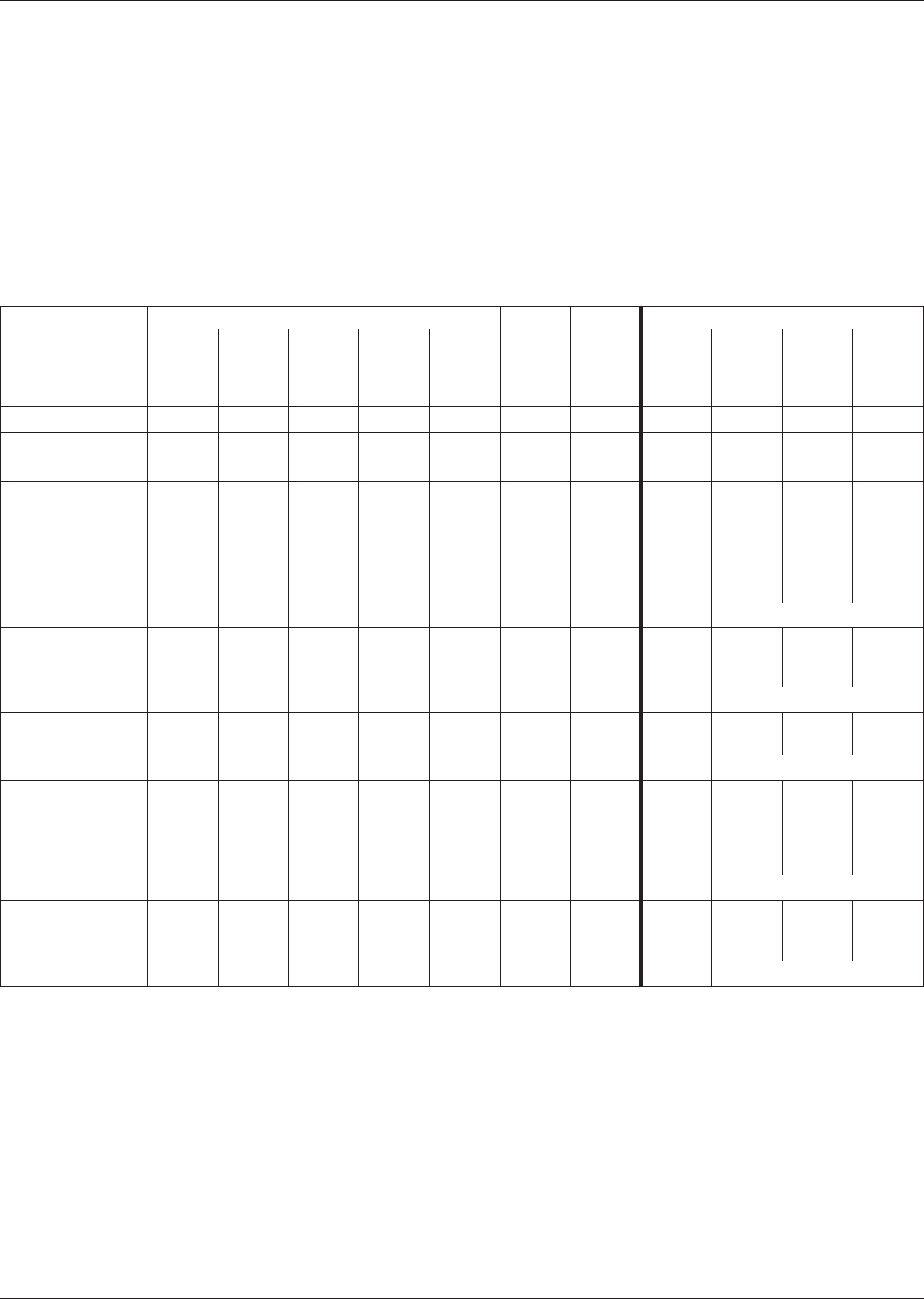
Table 3–6 Worst-Case Environments and Appropriate Equivalent Accelerated Testing
USE CATEGORY
WORST-CASE USE ENVIRONMENT ACCELERATED TESTING
Tmin
°C
Tmax
°C
∆T
(1)
°C
t
D
hrs
Cycles/
year
Typical
Years
of
Service
Approx.
Accept.
Failure
Risk, %
Tmin
°C
Tmax
°C
∆T
(2)
°C
t
D
min
1) CONSUMER 0 +60 35 12 365 1-3 1 +25 +100 75 15
2) COMPUTERS +15 +60 20 2 1460 5 0.1 +25 +100 75 15
3) TELECOM - 40 +85 35 12 365 7-20 0.01 0 +100 100 15
4) COMMERCIAL
AIRCRAFT
-55 +95 20 12 365 20 0.001 0 +100 100 15
5) INDUSTRIAL &
AUTOMOTIVE
PASSENGER
COMPARTMENT
-55 +95 20
&40
&60
&80
12
12
12
12
185
100
60
20
10 0.1 0 +100 100 15
& COLD
(3)
6) MILITARY
GROUND &
SHIP
-55 +95 40
&60
12
12
100
265
10 0.1 0 +100 100 15
& COLD
(3)
7) SPACE leo
geo
-55 +95 3
to 100
1
12
8760
365
5-30 0.001 0 +100 100 15
& COLD
(3)
8) MILITARY
AVIONICS a
b
c
-55 +95 40
60
80
&20
2
2
2
1
365
365
365
365
10 0.01 0 +100 100 15
& COLD
(3)
9) AUTOMOTIVE
UNDER HOOD
-55 +125 60
&100
&140
1
1
2
1000
300
40
5 0.1 0 +100 100 15
& COLD
(3)
& LARGE ∆T
(4)
& = in addition
1) ∆T represents the maximum temperature swing, but does not include power dissipation effects; for power dissipation calculate ∆T;
power dissipation can make pure temperature cycling accelerated testing significantly inaccurate. It should be noted that the cyclic
temperature range, ∆T, is not the difference between the possible minimum, T
MIN
, and maximum, T
MAX
, operational temperature
extremes; ∆T is typically significantly less.
2) All accelerated test cycles shall have temperature ramps <20°C/minute and dwell times at temperature extremes shall be 15 min-
utes measured on the test boards. This will give ~24 test cycles/day.
3) The failure/damage mechanism for solder changes at lower temperatures; for assemblies seeing significant cold environment
operations, additional ‘‘COLD’’ cycling, from perhaps –40 to 0°C, with dwell times long enough for temperature equilibration and for
a number of cycles equal to the ‘‘COLD’’ °C operational cycles in actual use is recommended.
4) The failure/damage mechanism for solder is different for large cyclic temperature swings traversing the stress-to-strain –20 to
+20°C transition region; for assemblies seeing such cycles in operation, additional appropriate ‘‘LARGE ∆T’’ testing with cycles
similar in nature and number to actual use is recommended.
December 1999 IPC-SM-782A
19
电子技术应用 www.ChinaAET.com