IPC-SM-782A 表面安装设计和焊盘设计标准(带BGA).pdf - 第28页
3.6 Design Rules During the component selection phase of a design, manufacturing engineering should be consulted regarding any components outside the scope of this docu- ment. The printed board design principles are a st…
3.5.3 Service Life
The design service life, N, can vary
significantly for the use categories in Table 3–6. The design
service lives can range from less than one year, barely
exceeding the warranty period for consumer products, to
20 years or more for telecommunications equipment and
commercial aircraft. For some military applications the ser-
vice life is measured in thousands of hours.
3.5.4 Acceptable Cumulative Failure Probability
The
acceptable cumulative failure probability, F(N), at the end
of the design service life, N, can vary significantly depend-
ing on the specific purpose of the product, the complexity
(number and mix of components) of the product, and per-
haps the design service life. F(N) values could range from
1 ppm for products whose failure has critical conse-
quences, e.g., cardiac pacemakers, to perhaps 10,000 ppm
(1%) for consumer products or products which provide
redundancy or ‘‘limp-home capability’’ in case of electrical
system failure. (See IPC-SM-785).
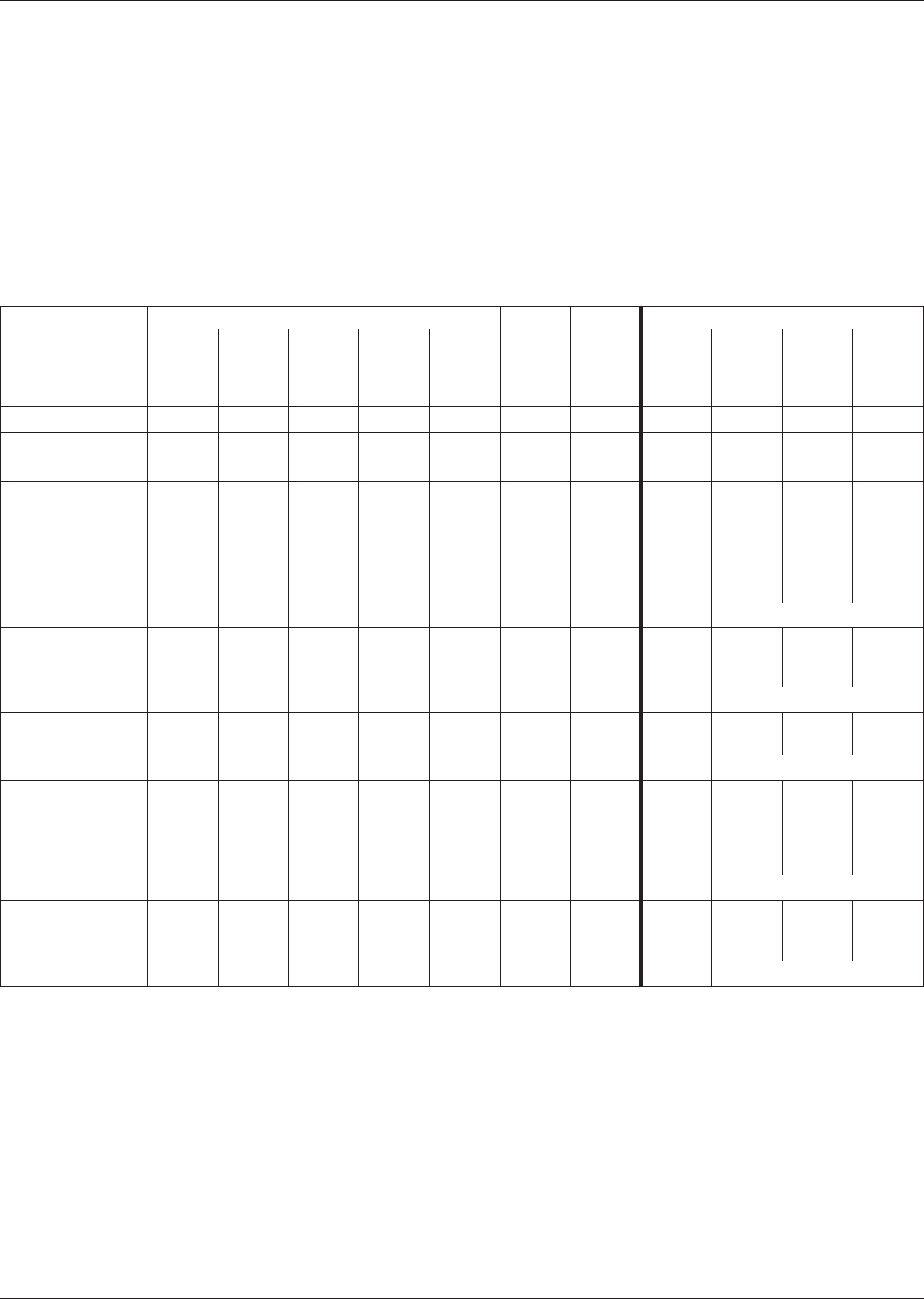
Table 3–6 Worst-Case Environments and Appropriate Equivalent Accelerated Testing
USE CATEGORY
WORST-CASE USE ENVIRONMENT ACCELERATED TESTING
Tmin
°C
Tmax
°C
∆T
(1)
°C
t
D
hrs
Cycles/
year
Typical
Years
of
Service
Approx.
Accept.
Failure
Risk, %
Tmin
°C
Tmax
°C
∆T
(2)
°C
t
D
min
1) CONSUMER 0 +60 35 12 365 1-3 1 +25 +100 75 15
2) COMPUTERS +15 +60 20 2 1460 5 0.1 +25 +100 75 15
3) TELECOM - 40 +85 35 12 365 7-20 0.01 0 +100 100 15
4) COMMERCIAL
AIRCRAFT
-55 +95 20 12 365 20 0.001 0 +100 100 15
5) INDUSTRIAL &
AUTOMOTIVE
PASSENGER
COMPARTMENT
-55 +95 20
&40
&60
&80
12
12
12
12
185
100
60
20
10 0.1 0 +100 100 15
& COLD
(3)
6) MILITARY
GROUND &
SHIP
-55 +95 40
&60
12
12
100
265
10 0.1 0 +100 100 15
& COLD
(3)
7) SPACE leo
geo
-55 +95 3
to 100
1
12
8760
365
5-30 0.001 0 +100 100 15
& COLD
(3)
8) MILITARY
AVIONICS a
b
c
-55 +95 40
60
80
&20
2
2
2
1
365
365
365
365
10 0.01 0 +100 100 15
& COLD
(3)
9) AUTOMOTIVE
UNDER HOOD
-55 +125 60
&100
&140
1
1
2
1000
300
40
5 0.1 0 +100 100 15
& COLD
(3)
& LARGE ∆T
(4)
& = in addition
1) ∆T represents the maximum temperature swing, but does not include power dissipation effects; for power dissipation calculate ∆T;
power dissipation can make pure temperature cycling accelerated testing significantly inaccurate. It should be noted that the cyclic
temperature range, ∆T, is not the difference between the possible minimum, T
MIN
, and maximum, T
MAX
, operational temperature
extremes; ∆T is typically significantly less.
2) All accelerated test cycles shall have temperature ramps <20°C/minute and dwell times at temperature extremes shall be 15 min-
utes measured on the test boards. This will give ~24 test cycles/day.
3) The failure/damage mechanism for solder changes at lower temperatures; for assemblies seeing significant cold environment
operations, additional ‘‘COLD’’ cycling, from perhaps –40 to 0°C, with dwell times long enough for temperature equilibration and for
a number of cycles equal to the ‘‘COLD’’ °C operational cycles in actual use is recommended.
4) The failure/damage mechanism for solder is different for large cyclic temperature swings traversing the stress-to-strain –20 to
+20°C transition region; for assemblies seeing such cycles in operation, additional appropriate ‘‘LARGE ∆T’’ testing with cycles
similar in nature and number to actual use is recommended.
December 1999 IPC-SM-782A
19
电子技术应用 www.ChinaAET.com
3.6 Design Rules
During the component selection phase
of a design, manufacturing engineering should be consulted
regarding any components outside the scope of this docu-
ment.
The printed board design principles are a statement of cur-
rent test and manufacturing capabilities. Exceeding or
changing these capabilities requires concurrence of all par-
ticipants in the process including manufacturing, engineer-
ing and test technology.
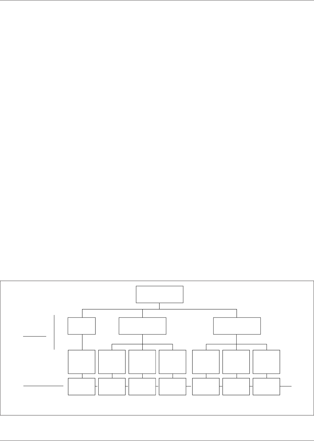
Involving test and manufacturing early in the design helps
to move a quality product quickly into production. Figure
3–7 shows a list of concurrent engineering team partici-
pants that should be involved.
3.6.1 Component Spacing
3.6.1.1 Component Considerations
The land pattern
design information discussed so far is important for reli-
ability of surface mount assemblies. However, the designer
should not lose sight of manufacturability, testability and
repairability of SMT assemblies. A minimum interpackage
spacing is required to satisfy all these manufacturing
requirements. There is no limit on maximum interpackage
spacing; the more the better. Some designs require that sur-
face mount components are positioned as tightly as pos-
sible. Based on experience, the examples shown in Figure
3–8 meet manufacturability requirements.
The land to land spacing between adjacent components
should be 1.25 mm [0.050 in] clear space all around the
edges of printed boards if boards are tested off the connec-
tor or 2.5 mm [0.100 in] minimum if vacuum seal for test-
ing is used. The requirements specified herein are recom-
mended minimums excluding conductor geometry
tolerances.
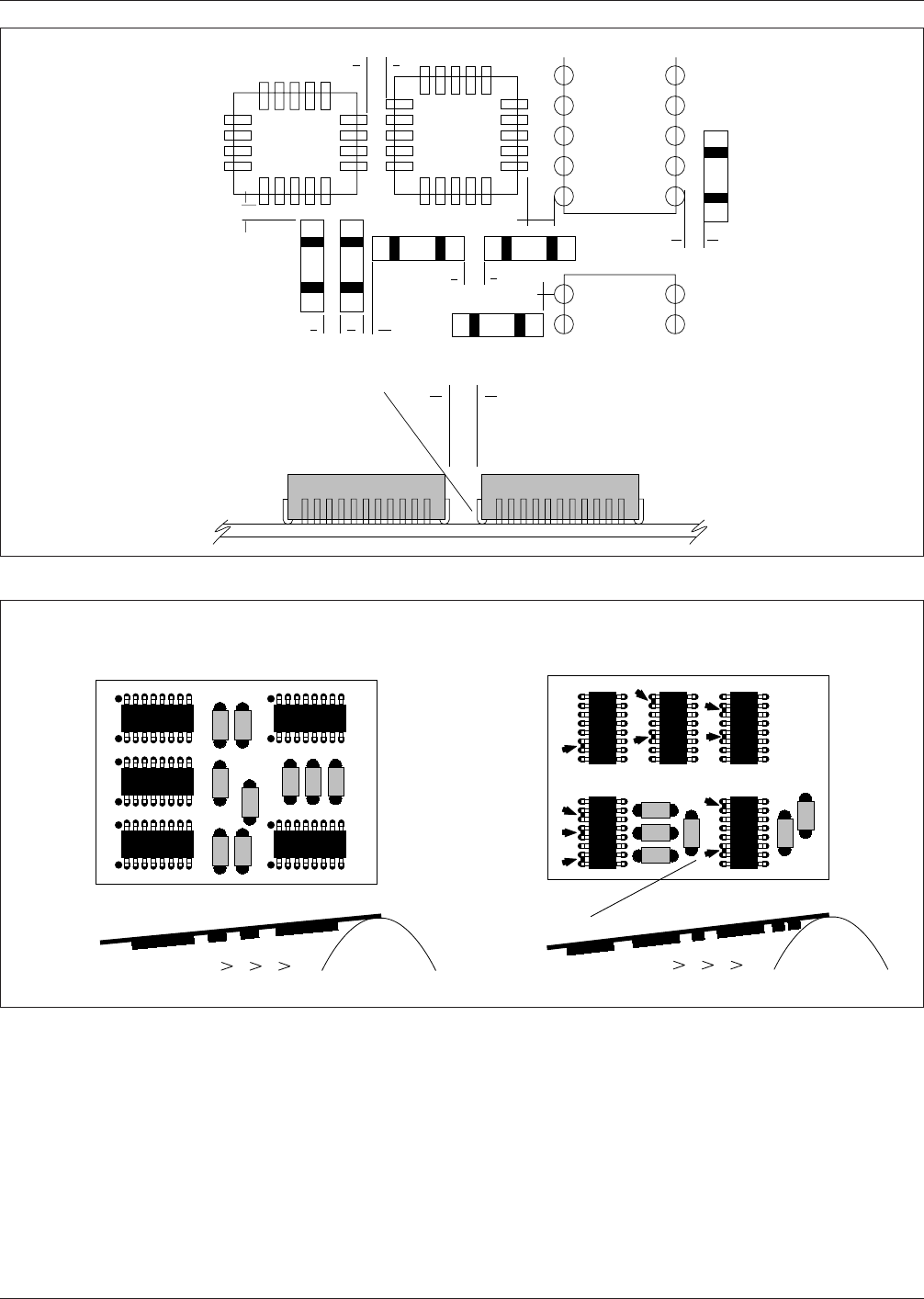
3.6.1.2 Wave Solder Component Orientation
All polar-
ized surface mount components should be placed in the
same orientation, when possible. On any printed board
assembly where the secondary side is to be wave soldered,
the preferred orientation of devices on that side is
described and shown in Figure 3–9. The preferred orienta-
tion is used in order to optimize the resulting solder joint
quality as the assembly exits the solder wave.
• All passive components shall be parallel to each other.
• All SOICs shall be perpendicular to the long axis of
passive components.
• The longer axis of SOICs and of passive components
shall be perpendicular to each other.
• The long axis of passive components shall be perpen-
dicular to the direction of travel of the board along
the conveyer of the wave solder machine.
3.6.1.3 Component Placement
Similar types of compo-
nents should be aligned on the board in the same orienta-
tion for ease of component placement, inspection, and sol-
dering. Also, similar component types should be grouped
together whenever possible, with the net list or connectiv-
ity and circuit performance requirements ultimately driving
the placements. See Figure 3-10. In memory boards, for
example, all of the memory chips are placed in a clearly
defined matrix with pin one orientation the same direction
for all components. This is a good design practice to carry
out on logic designs where there are many similar compo-
nent types with different logic functions in each package.
On the other hand, analog designs often require a large
variety of component types making it understandably diffi-
cult to group similar components together. Regardless if
IPC-782-3-7
Figure 3–7 Simplified electronic development organization
▼
▼
▼
▼
▼
▼
▼
▼
▼
Admin-
istrative
control
Chain of
command
Operational
control
Working
level
PROGRAM
OFFICE
System
Manage-
ment
Project
Task
MANAGEMENT
ENGINEERING
MANAGEMENT
System
Engin-
eering
Elec-
tronic
Design
MANUFACTURING
MANAGEMENT
Product
Design
Fabri-
cation
Assem-
bly
Testing
Project
Task
Project
Task
Project
Task
Project
Task
Project
Task
Project
Task
Deliverable
Hardware
IPC-SM-782A December 1999
20
电子技术应用 www.ChinaAET.com
the design is memory, general logic, or analog, it is recom-
mended that all component orientations are such that pin
one orientation is the same.
3.6.1.4 Grid-Based Component Placement
SMT com-
ponent placement and orientation is generally more difficult
than THT printed boards for two reasons: higher compo-
nent densities, and the ability to put components on both
sides of the board. For THT designs, the component leads
are on 2.54 mm [0.100 in] centers and, assuming 1.3 mm
[0.065 in] lands, the spacing between lands would be 1.2
mm. In high density SMT designs, however, the spacing
between lands is often less, down to 0.63 mm [0.025 in]
and smaller. Grid based component placement (0.100 inch
grid is standard with THT) is complicated by the large
variety of land sizes associated with the SMT component
packages now becoming available. Most SMT designs
being done today have abandoned the 2.54 mm [0.100 in]
IPC-782-3-8
Figure 3–8 Recommended minimum land-to-land clearances
Maximize View
Angle
for
Solder
Joint
Inspection
2.5 mm (0.100 in) Minimum
▼
▼
▼
▼
▼
▼
▼
1.25 mm (0.050 in)
1.5 mm (0. 060 in.)
0.63 mm (0.025 in.)
1.0 mm (0.040 in.)
1.0 mm
(0.040 in.)
▼
▼
▼
▼
▼
▼
0.63 mm
(0.025 in.)
1.25 mm
(0.050 in)
1.5 mm (0.060 in.)
▼
▼
▼
▼
▼
DIP
IPC-782-3-9
Figure 3–9 Component orientation for wave solder applications
Wave Solder For SMT
Prefered IC orientation
Rubber pads will reduce
solder bridging
Typical solder
bridge locations
▼
▼
Non Prefered IC orientation
December 1999 IPC-SM-782A
21
电子技术应用 www.ChinaAET.com