IPC-SM-782A 表面安装设计和焊盘设计标准(带BGA).pdf - 第69页
1.0 INTRODUCTION This section covers land patterns for various discrete compo- nents. Each subsection contains information in accordance with the following format: 1.0 Scope 2.0 Applicable Documents 3.0 General Component…

Tolerance Analysis
Page 4 shows the details of the tolerance analysis of the component and land pattern shown in the data set. The first two
columns of the table show the board fabrication allowances in the analysis; the second column shows the allowances used
to represent placement registration in terms of DTP (diameter of true position), with the point of origin being the center of
the land pattern.
The next part of the analysis provides three pieces of information for the toe fillet, heel fillet, and side fillet. The first part
of the set is the range of differences between maximum and minimum component dimensions. These are: the overall dimen-
sion (usually ‘‘L’’) identified as ‘‘C’’; the inside dimension l (usually ‘‘S’’) identified as ‘‘C’’; and the side or lead width s
(usually ‘‘W’’) identified as ‘‘C.’’ The second and third columns w of each triplet set show the minimum and maximum sta-
tistically derived solder fillet opportunity. These two columns become the upper and lower specification limits for any sta-
tistical process control (SPC) analysis. If these conditions are not met, something has shifted in the process, or the parts
being assembled in the process.
Revision Status
The following is the revision status of the component family data sets of IPC-SM-782A. A dash (‘‘-‘‘) signifies that the sec-
tion is the original release; the letter ‘‘A’’ after the section number refers to the first revision to the four-page set; the letter
‘‘B’’ refers to the second revision, etc.
Section Revision
Number Status Section Title
8.0 — Discrete Components
8.1 A Chip Resistors
8.2 A Chip Capacitors
8.3 — Inductors
8.4 A Tantalum Capacitors
8.5 A Metal Electrode Face (MELF) Components
8.6 — Small Outline Transistor (SOT) 23
8.7 — Small Outline Transistor (SOT) 89
8.8 A Small Outline Diode (SOD) 123
8.9 — Small Outline Transistor (SOT) 143
8.10 — Small Outline Transistor (SOT) 223
8.11 A Modified Through-Hole Component (TO) 252
9.0 — Components with Gullwing Leads on Two Sides—
9.1 A Small Outline Integrated Circuits (SOIC)
9.2 A Small Outline Integrated Circuits (SSOIC)
9.3 A Small Outline Package Integrated Circuit (SOPIC)
9.4 A Thin Small Outline Package
9.5 — Ceramic Flat Pack (CFP)
10.0 — Components with J Leads on Two Sides
10.1 A Small Outline Integrated Circuits with J Leads (SOJ)—7.63 mm [0.300] Body Size
10.2 — Small Outline Integrated Circuits with J Leads (SOJ)—8.88 mm [0.350] Body Size
10.3 — Small Outline Integrated Circuits with J Leads (SOJ)—10.12 mm [0.400] Body Size
10.4 — Small Outline Integrated Circuits with J Leads (SOJ)—11.38 mm [0.450] Body Size
11.0 — Components with Gullwing Leads on Four Sides
11.1 A Plastic Quad Flat Pack (PQFP)
11.2 A Shrink Quad Flat Pack (SQFP), Square
11.3 A Shrink Quad Flat Pack (SQFP), Rectangular
11.4 A Ceramic Quad Flat Pack (CQFP)
12.0 — Components with J Leads on Four Sides
12.1 A Plastic Leaded Chip Carrier (PLCC), Square
12.2 A Plastic Leaded Chip Carrier (PLCC), Rectangular
12.3 — Leadless Ceramic Chip Carrier (LCC)
13.0 — Modified Dual-In-Line Pin (DIP) Components
13.1 — DIP
14.0 – Components with Ball Grid Array Contacts
14.1 – Plastic Ball Grid Array
14.2 – 1.27 mm Pitch Rectangular PBGA JEDEC MS-028
IPC-SM-782A December 1999
60
电子技术应用 www.ChinaAET.com
1.0 INTRODUCTION
This section covers land patterns for various discrete compo-
nents. Each subsection contains information in accordance
with the following format:
1.0 Scope
2.0 Applicable Documents
3.0 General Component Description (Figure 1)
4.0 Component Dimensions (Figure 2)
5.0 Land Pattern Dimensions (Figure 3)
6.0 Tolerance and Solder Joint Analysis (Figure 4)
The following is the table of contents for this section:
Table of Contents
Rectangular Leadless Components
Section Component
8.1 Chip Resistors
8.2 Chip Capacitors
8.3 Inductors
8.4 Tantalum Capacitors
Circular Leadless Components
Section Component
8.5 MELF (Metal Electrode Face) Resistors and Diodes
Small Outline Transistors (SOT) and Diodes (SOD)
Section Component
8.6 SOT 23
8.7 SOT 89
8.8 SOD 123
8.9 SOT 143
8.10 SOT 223
Modified Through-Hole (TO) Packs
for Transistors and Diodes
Section Component
8.11 TO 252
2.0 APPLICABLE DOCUMENTS
The following documents, of the issue in effect on the revision
date of this section, form a part of this specification to the
extent specified herein.
2.1 Electronic Industries Association (EIA)
1
EIA-PDP-100
Registered and Standard Mechanical Outlines
for Electronic Parts
EIA-481-A
Taping of Surface Mount Components for Auto-
matic Placement
EIA-481-1
8 mm and 2 mm Taping of Surface Mount Com-
ponents for Automatic Handling
EIA-481-2
16 mm and 24 mm Embossed Carrier Taping of
Surface Mount Components for Automated Handling
EIA-481-3
32 mm, 44 mm, and 56 mm Embossed Carrier
Taping of Surface Mount Components for Automated Han-
dling
2.2 International Electrotechnical Commission (IEC)
2
IEC 97
Grid System for Printed Circuits
3.0 GENERAL INFORMATION
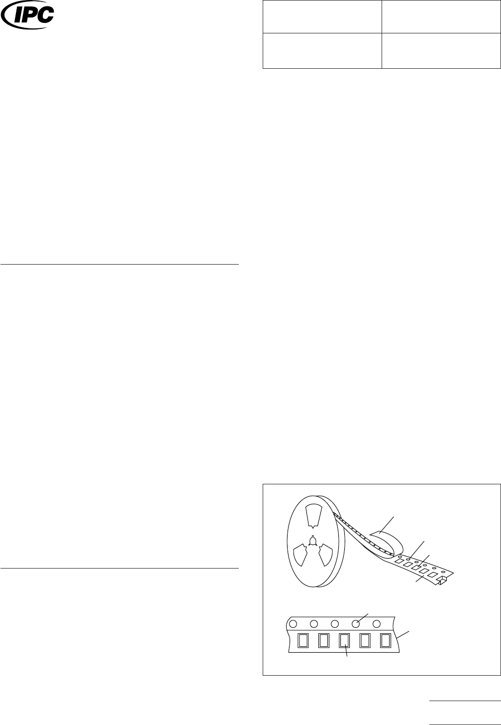
3.1 Packaging
Discrete components are generally pur-
chased in 8 mm and 12 mm wide tape and reel. See Figure
1. EIA-481 is the applicable specification for tape and reel.
Consult your manufacturers guide for the packaging availabil-
ity of your component.
Parts susceptible to damage by electrostatic discharge shall
be supplied in a manner that prevents such damage. Tape
peel strength shall be 40 ±30 grams. Peel from the top for the
top cover of the tape. Reel materials used in the construction
of the reel shall be easily disposable metal, chip board, sty-
rene plastic or equivalent. Reels shall not cause deterioration
of the components or their solderability. Reels must be able to
withstand high humidity conditions.
IPC-782-8-0-1
Figure 1 Packaging
Top cover tape
Sprocket hole
Component cavity
Embossed carrier tape
Sprocket hole
Embossed carrier tape
Component cavity
▼
▼
▼
▼
▼
▼
▼
IPC-SM-782
Surface Mount Design
and Land Pattern Standard
Date
8/93
Section
8.0
Revision Subject
Discrete Components
Page1of2
电子技术应用 www.ChinaAET.com

3.2 Resistance to Cleaning Processes
Parts must be
capable of withstanding cleaning processes currently used by
board assembly manufacturers. This may include as a mini-
mum 4-minute exposures to solvent cleaning solutions at
40°C, plus a minimum of a 1-minute exposure to ultrasonic
immersion at a frequency of 40 kHz and a power of 100 watts
per square foot. Alkaline systems in use shall also not damage
parts or remove markings.
1. Application for copies should be addressed to EIA, 2001
Pennsylvania Ave N.W., Washington, DC, 20006-1813 or
Global Engineering Documents, 1990 M St. N.W., Wash-
ington, DC 20036.
2. Application for copies should be addressed to IEC, 3 rue
de Varembe, PO Box 131—1211 Geneva 20, Switzerland
IPC-SM-782
Subject
Discrete Components
Date
8/93
Section
8.0
Revision
Page2of2
电子技术应用 www.ChinaAET.com