IPC-SM-782A 表面安装设计和焊盘设计标准(带BGA).pdf - 第70页
3.2 Resistance to Cleaning Processes Parts must be capable of withstanding cleaning processes currently used by board assembly manufacturers. This may include as a mini- mum 4-minute exposures to solvent cleaning solutio…
1.0 INTRODUCTION
This section covers land patterns for various discrete compo-
nents. Each subsection contains information in accordance
with the following format:
1.0 Scope
2.0 Applicable Documents
3.0 General Component Description (Figure 1)
4.0 Component Dimensions (Figure 2)
5.0 Land Pattern Dimensions (Figure 3)
6.0 Tolerance and Solder Joint Analysis (Figure 4)
The following is the table of contents for this section:
Table of Contents
Rectangular Leadless Components
Section Component
8.1 Chip Resistors
8.2 Chip Capacitors
8.3 Inductors
8.4 Tantalum Capacitors
Circular Leadless Components
Section Component
8.5 MELF (Metal Electrode Face) Resistors and Diodes
Small Outline Transistors (SOT) and Diodes (SOD)
Section Component
8.6 SOT 23
8.7 SOT 89
8.8 SOD 123
8.9 SOT 143
8.10 SOT 223
Modified Through-Hole (TO) Packs
for Transistors and Diodes
Section Component
8.11 TO 252
2.0 APPLICABLE DOCUMENTS
The following documents, of the issue in effect on the revision
date of this section, form a part of this specification to the
extent specified herein.
2.1 Electronic Industries Association (EIA)
1
EIA-PDP-100
Registered and Standard Mechanical Outlines
for Electronic Parts
EIA-481-A
Taping of Surface Mount Components for Auto-
matic Placement
EIA-481-1
8 mm and 2 mm Taping of Surface Mount Com-
ponents for Automatic Handling
EIA-481-2
16 mm and 24 mm Embossed Carrier Taping of
Surface Mount Components for Automated Handling
EIA-481-3
32 mm, 44 mm, and 56 mm Embossed Carrier
Taping of Surface Mount Components for Automated Han-
dling
2.2 International Electrotechnical Commission (IEC)
2
IEC 97
Grid System for Printed Circuits
3.0 GENERAL INFORMATION
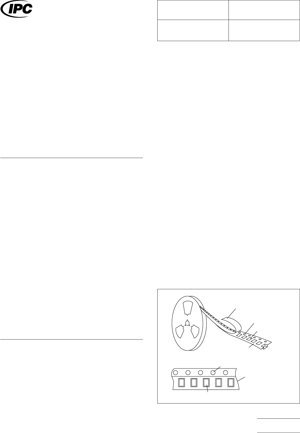
3.1 Packaging
Discrete components are generally pur-
chased in 8 mm and 12 mm wide tape and reel. See Figure
1. EIA-481 is the applicable specification for tape and reel.
Consult your manufacturers guide for the packaging availabil-
ity of your component.
Parts susceptible to damage by electrostatic discharge shall
be supplied in a manner that prevents such damage. Tape
peel strength shall be 40 ±30 grams. Peel from the top for the
top cover of the tape. Reel materials used in the construction
of the reel shall be easily disposable metal, chip board, sty-
rene plastic or equivalent. Reels shall not cause deterioration
of the components or their solderability. Reels must be able to
withstand high humidity conditions.
IPC-782-8-0-1
Figure 1 Packaging
Top cover tape
Sprocket hole
Component cavity
Embossed carrier tape
Sprocket hole
Embossed carrier tape
Component cavity
▼
▼
▼
▼
▼
▼
▼
IPC-SM-782
Surface Mount Design
and Land Pattern Standard
Date
8/93
Section
8.0
Revision Subject
Discrete Components
Page1of2
电子技术应用 www.ChinaAET.com

3.2 Resistance to Cleaning Processes
Parts must be
capable of withstanding cleaning processes currently used by
board assembly manufacturers. This may include as a mini-
mum 4-minute exposures to solvent cleaning solutions at
40°C, plus a minimum of a 1-minute exposure to ultrasonic
immersion at a frequency of 40 kHz and a power of 100 watts
per square foot. Alkaline systems in use shall also not damage
parts or remove markings.
1. Application for copies should be addressed to EIA, 2001
Pennsylvania Ave N.W., Washington, DC, 20006-1813 or
Global Engineering Documents, 1990 M St. N.W., Wash-
ington, DC 20036.
2. Application for copies should be addressed to IEC, 3 rue
de Varembe, PO Box 131—1211 Geneva 20, Switzerland
IPC-SM-782
Subject
Discrete Components
Date
8/93
Section
8.0
Revision
Page2of2
电子技术应用 www.ChinaAET.com
1.0 SCOPE
Microminiature leadless devices are available to the circuit
designer in rectangular form for discrete components such as
chip resistors.
This subsection provides the component and land pattern
dimensions for chip resistors, along with an analysis of toler-
ance and solder joint assumptions used to arrive at the land
pattern dimensions. Basic construction of the chip resistor is
also covered.
2.0 APPLICABLE DOCUMENTS
See Section 8.0 for documents applicable to the subsections.
3.0 COMPONENT DESCRIPTIONS
A variety of values exist for resistors. The following sections
describe the most common types.
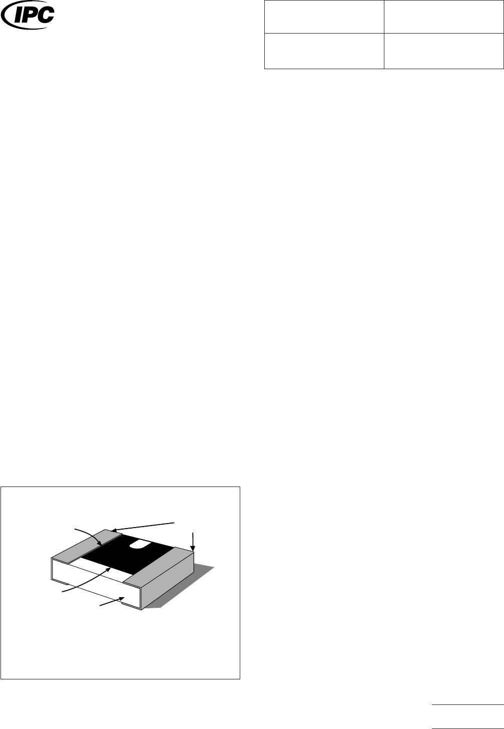
3.1 Basic Construction
The resistive material is applied to
a ceramic substrate and terminated symmetrically at both
ends with a ‘‘wrap around’’ metal U-shaped band. The resis-
tive material is face-up, thus trimming to close tolerances is
possible. Since most equipment uses a vacuum-type pickup
head, it is important that the surface of the resistor is made flat
after trimming, otherwise vacuum pickup might be difficult.
See Figure 1.
3.1.1 Termination Materials
End terminations should be
solder coated with a tin/lead alloy. The solder should contain
between 58 to 68% tin. Solder may be applied to the termi-
nation by hot dipping or by plating from solution. Plated sol-
der terminations should be subjected to a post-plating reflow
operation to fuse the solder. The tin/lead finish should be at
least 0.0075 mm [0.0003 in.] thick.
The termination shall be symmetrical, and shall not have nod-
ules lumps, protrusions, etc., that compromise the symmetry
or dimensional tolerances of the part. The end termination
shall cover the ends of the components, and shall extend out
to the top and bottom of the component.
Solder finish applied over precious metal electrodes shall have
a diffusion-barrier layer between the electrode metalization
and the solder finish. The barrier layer should be nickel or an
equivalent diffusion barrier, and should be at least 0.00125
mm [0.00005 in] thick.
3.1.2 Marking
Resistors equal to or larger than 2012
[0805] are labeled. Resistors smaller than 1608 [0603] are
generally unlabeled.
3.1.3 Carrier Package Format
Bulk rods, 8 mm tape/4
mm pitch is preferred for best handling. Tape and reel speci-
fications provide additional requirements.
3.1.4 Resistance to Soldering
Parts should be capable of
withstanding five cycles through a standard reflow system
operating at 215°C. Each cycle shall consist of 60 seconds
exposure at 215°C. Parts must also be capable of withstand-
ing a minimum of 10 seconds immersion in molten solder at
260°C.
IPC-782-8-1-1
Figure 1 Chip resistor construction
Resistor
Alumina Chip
Platinum-silver
Wrap-around
termination
Wire Bond Construction
Glass
Passivation
IPC-SM-782
Surface Mount Design
and Land Pattern Standard
Date
5/96
Section
8.1
Revision
A
Subject
Chip Resistors
Page1of4
电子技术应用 www.ChinaAET.com