IPC-SM-782A 表面安装设计和焊盘设计标准(带BGA).pdf - 第80页
4.0 COMPONENT DIMENSIONS Figure 2 provides the component dimensions for inductors. Component Identifier (mm) L (mm) S (mm) W1 (mm) W2 (mm) T (mm) H1 (mm) H2 (mm) min max min max min max min max min max max max 2012 Chip 1…
1.0 SCOPE
Microminiature leadless devices are available to the circuit
designer in rectangular form for discrete components such as
inductors.
This subsection provides the component and land pattern
dimensions for inductors, along with an analysis of tolerance
and solder joint assumptions used to arrive at the land pattern
dimensions. Basic construction of the inductor is also cov-
ered.
2.0 APPLICABLE DOCUMENTS
See Section 8.0 for documents applicable to the subsections.
3.0 COMPONENT DESCRIPTIONS
A variety of values exist for inductors. The following sections
describe the most common types.
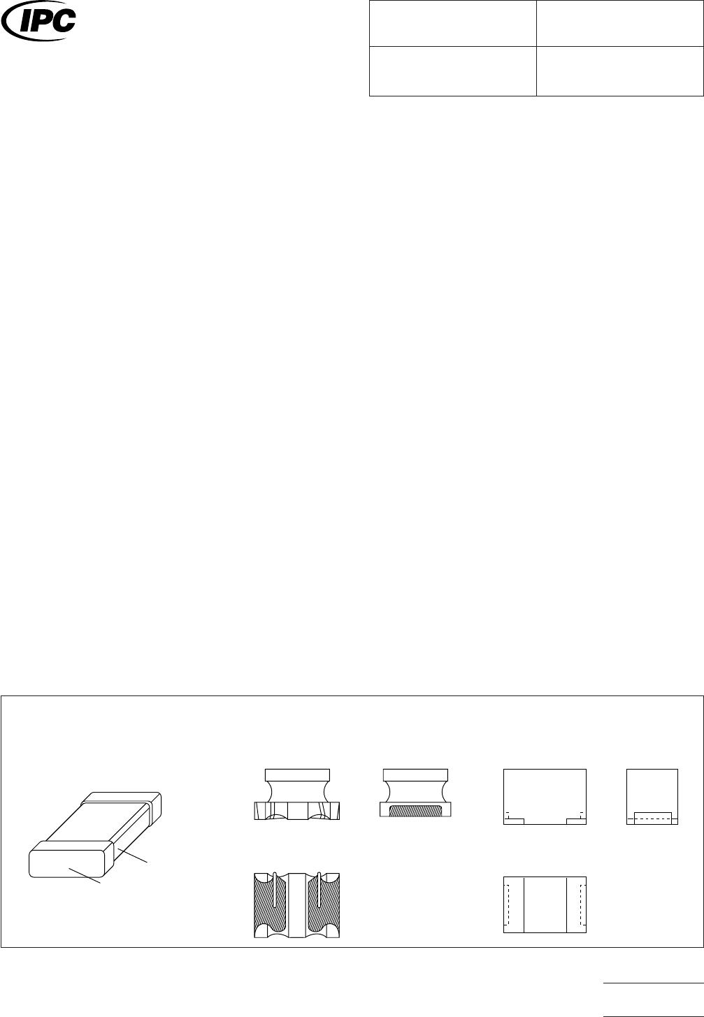
3.1 Basic Construction
At the time of publication, there
was no industry standard document for leadless inductors.
The dimensions were taken from manufacturer’s catalogs, but
only when at least two component vendors manufacture the
same package. However, the same inductor value may not be
available in the same package from the two manufacturers.
See Figure 1.
3.1.1 Termination Materials
End terminations should be
solder coated with a tin/lead alloy. The solder should contain
between 58 to 68% tin. Solder may be applied to the termi-
nation by hot dipping or by plating from solution. Plated sol-
der
terminations should be subjected to a post-plating reflow
operation to fuse the solder. The tin/lead finish should be at
least 0.0075 mm [0.0003 in] thick.
The termination shall be symmetrical, and shall not have nod-
ules lumps, protrusions, etc., that compromise the symmetry
or dimensional tolerances of the part. The end termination
shall cover the ends of the components, and shall extend out
to the top and bottom of the component.
Most common termination materials include palladium-silver
alloy, silver, and gold. Solder finish applied over precious
metal electrodes shall have a diffusion-barrier layer between
the electrode metallization and the solder finish. The barrier
layer should be nickel or an equivalent diffusion barrier, and
should be at least 0.00125 mm [0.00005 in] thick.
3.1.2 Marking
Parts are available with or without marked
inductance values.
3.1.3 Carrier Package Format
Bulk rods, 8 mm tape/4
mm pitch is preferred for best handling. Tape and reel speci-
fications provide additional requirements.
3.1.4 Resistance to Soldering
Parts should be capable of
withstanding five cycles through a standard reflow system
operating at 215°C. Each cycle shall consist of 60 seconds
exposure at 215°C. Parts must also be capable of withstand-
ing a minimum of 10 seconds immersion in molten solder at
260°C.
IPC-782-8-3-1
Figure 1 Inductor construction
Ferrite
Chip
▼
Precision wire—wound Molded
External electrode
▼
IPC-SM-782
Surface Mount Design
and Land Pattern Standard
Date
8/93
Section
8.3
Revision Subject
Inductors
Page1of4
电子技术应用 www.ChinaAET.com
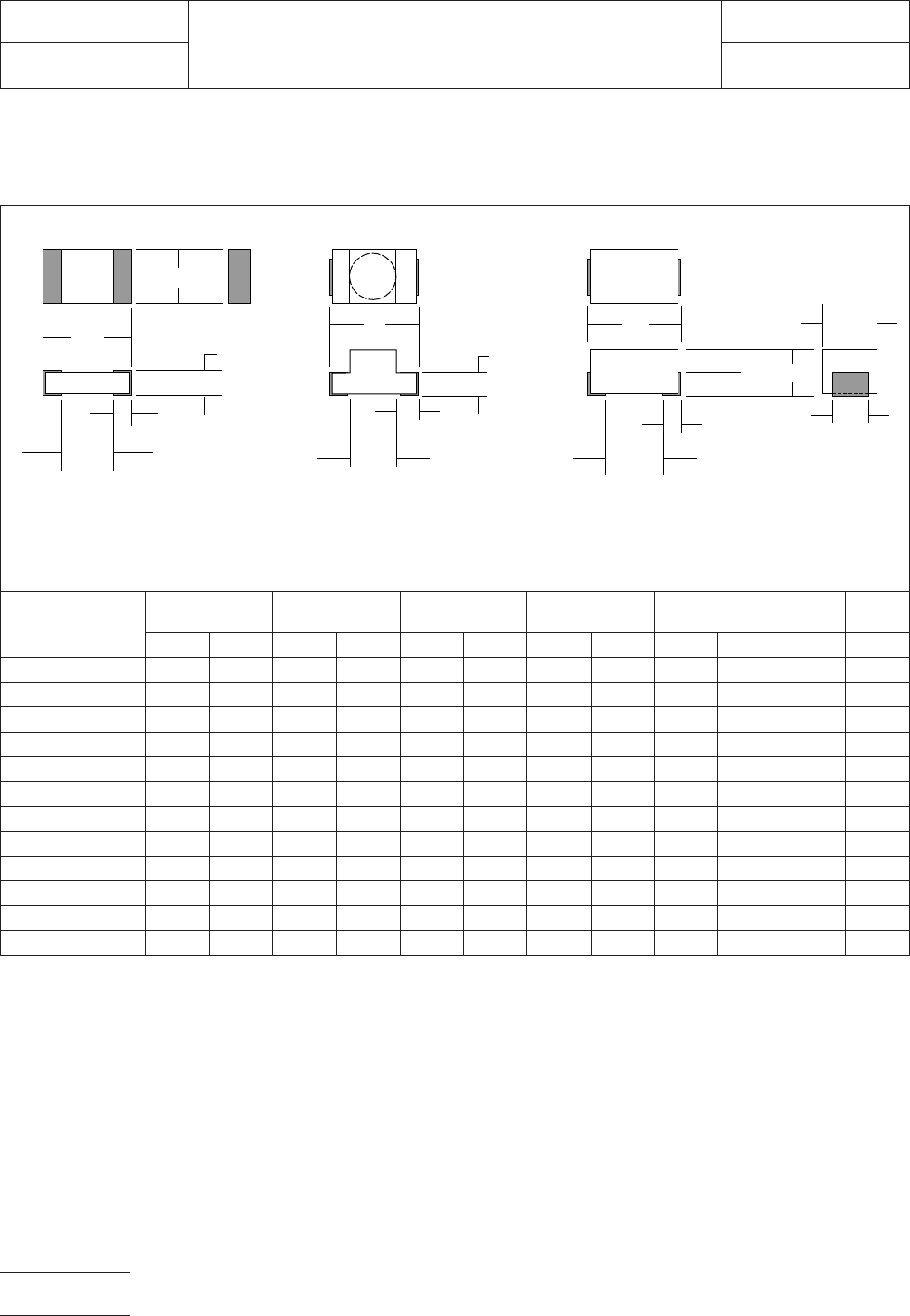
4.0 COMPONENT DIMENSIONS
Figure 2 provides the component dimensions for inductors.
Component
Identifier (mm)
L (mm) S (mm) W1 (mm) W2 (mm) T (mm)
H1
(mm)
H2
(mm)
min max min max min max min max min max max max
2012 Chip 1.70 2.30 1.10 1.76 0.60 1.20 — — 0.10 0.30 1.20 —
3216 Chip 2.90 3.50 1.90 2.63 1.30 1.90 — — 0.20 0.50 1.90 —
4516 Chip 4.20 4.80 2.60 3.53 0.60 1.20 — — 0.30 0.80 1.90 —
2825 Prec. w/w 2.20 2.80 0.90 1.62 1.95 2.11 2.10 2.54 0.37 0.65 2.29 0.07
3225 Prec. w/w 2.90 3.50 0.90 1.83 1.40 1.80 — — 0.50 1.00 2.00 0.50
4532 Prec. w/w 4.20 4.80 2.20 3.13 3.00 3.40 — — 0.50 1.00 2.80 0.50
5038 Prec. w/w 4.35 4.95 2.81 3.51 2.46 2.62 3.41 3.81 0.51 0.77 3.80 0.76
3225/3230 Molded 3.00 3.40 1.60 2.18 1.80 2.00 2.30 2.70 0.40 0.70 2.40 0.51
4035 Molded 3.81 4.32 0.81 1.60 1.20 1.50 2.92 3.18 1.20 1.50 2.67 1.27
4532 Molded 4.20 4.80 2.30 3.15 2.00 2.20 3.00 3.40 0.65 0.95 3.40 0.50
5650 Molded 5.30 5.50 3.30 4.32 3.80 4.20 4.70 5.30 0.50 1.00 5.80 1.00
8530 Molded 8.25 8.76 5.25 6.04 1.20 1.50 2.92 3.18 1.20 1.50 2.67 1.27
Figure 2 Inductor component dimensions
Chip Precision wire - wound Molded
W
▼
▼
L
L
▼
▼
▼
▼
S
H1
▼
▼
▼
▼
T
H1
▼
▼
▼
▼
S
▼
▼
H2
▼
▼
T
▼
▼
S
L
▼
▼
▼
▼
T
▼
▼
W2
▼
▼
▼
W1
▼
▼
H2
▼
IPC-782-8-3-2
IPC-SM-782
Subject
Inductors
Date
8/93
Section
8.3
Revision
Page2of4
电子技术应用 www.ChinaAET.com
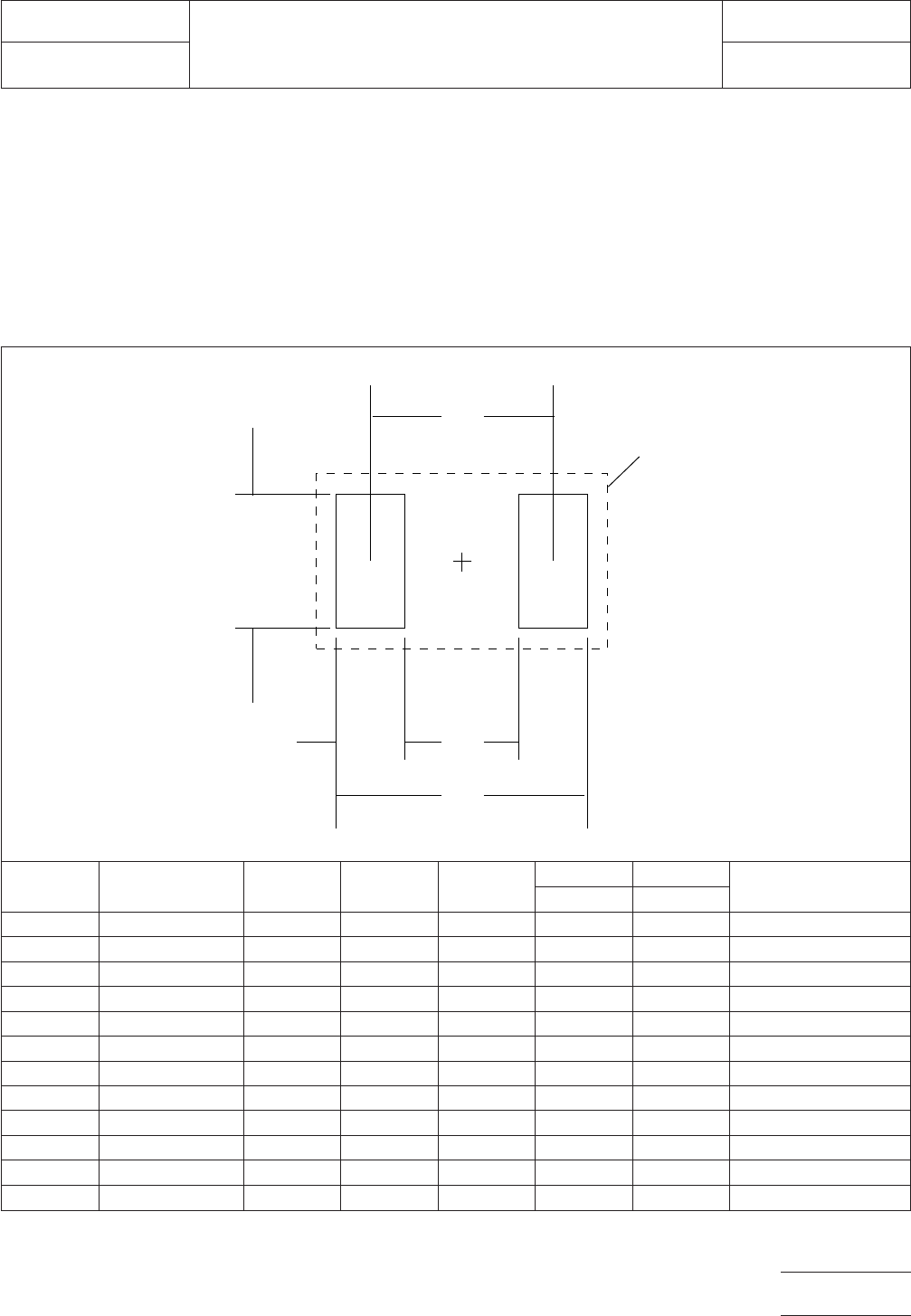
5.0 LAND PATTERN DIMENSIONS
Figure 3 provides the land pattern dimensions for inductors.
These numbers represent industry consensus on the best
dimensions based on empirical knowledge of fabricated land
patterns.
In the table, the dimensions shown are at maximum material
condition (MMC). The least mate-rial condition (LMC) should
not exceed the fabrication (F) allowance shown on page 4.
The LMC and the MMC provide the limits for each dimension.
The dotted line in Figure 3 shows the grid placement court-
yard which is the area required to place land patterns and
their respective components in adjacent proximity without
interference or shorting. Numbers in the table represent the
number of grid elements (each element is 0.5 by 0.5 mm) in
accordance with the international grid detailed in IEC publica-
tion 97.
RLP No.
Component
Identifier (mm) Z (mm) G (mm) X (mm)
C (mm) Y (mm)
Placement Grid
(No. Grid Elements)ref ref
160 2012 Chip 3.00 1.00 1.00 2.00 1.00 4x8
161 3216 Chip 4.20 1.80 1.60 3.00 1.20 6x10
162 4516 Chip 5.80 2.60 1.00 4.20 1.60 4x12
163 2825 Prec 3.80 1.00 2.40 2.40 1.40 6x10
164 3225 Prec 4.60 1.00 2.00 2.80 1.80 6x10
165 4532 Prec 5.80 2.20 3.60 4.00 1.80 8x14
166 5038 Prec 5.80 3.00 2.80 4.40 1.40 8x14
167 3225/3230 Molded 4.40 1.20 2.20 2.80 1.60 6x10
168 4035 Molded 5.40 1.00 1.40 3.20 2.20 8x12
169 4532 Molded 5.80 1.80 2.40 3.80 2.00 8x14
170 5650 Molded 6.80 3.20 4.00 5.00 1.80 12x16
171 8530 Molded 9.80 5.00 1.40 7.40 2.40 8x22
Figure 3 Inductor land pattern dimensions
▼
▼
▼
▼
▼
▼
▼
▼
▼
C
G
Z
X
Y
Grid
placement
courtyard
▼
IPC-782-8-3-3
IPC-SM-782
Subject
Inductors
Date
8/93
Section
8.3
Revision
Page3of4
电子技术应用 www.ChinaAET.com