IPC-SM-782A 表面安装设计和焊盘设计标准(带BGA).pdf - 第81页
5.0 LAND PATTERN DIMENSIONS Figure 3 provides the land pattern dimensions for inductors. These numbers represent industry consensus on the best dimensions based on empirical knowledge of fabricated land patterns. In the …
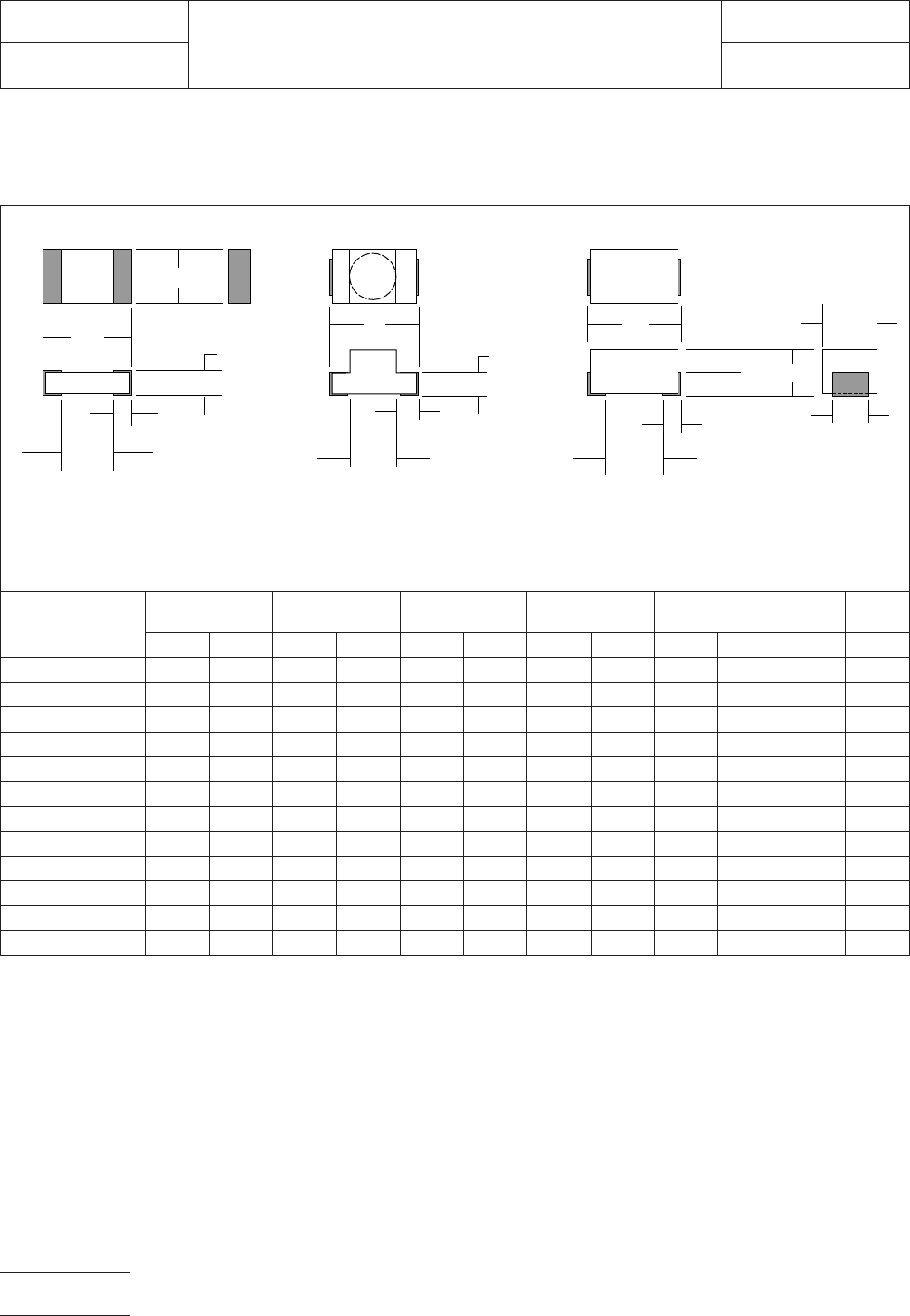
4.0 COMPONENT DIMENSIONS
Figure 2 provides the component dimensions for inductors.
Component
Identifier (mm)
L (mm) S (mm) W1 (mm) W2 (mm) T (mm)
H1
(mm)
H2
(mm)
min max min max min max min max min max max max
2012 Chip 1.70 2.30 1.10 1.76 0.60 1.20 — — 0.10 0.30 1.20 —
3216 Chip 2.90 3.50 1.90 2.63 1.30 1.90 — — 0.20 0.50 1.90 —
4516 Chip 4.20 4.80 2.60 3.53 0.60 1.20 — — 0.30 0.80 1.90 —
2825 Prec. w/w 2.20 2.80 0.90 1.62 1.95 2.11 2.10 2.54 0.37 0.65 2.29 0.07
3225 Prec. w/w 2.90 3.50 0.90 1.83 1.40 1.80 — — 0.50 1.00 2.00 0.50
4532 Prec. w/w 4.20 4.80 2.20 3.13 3.00 3.40 — — 0.50 1.00 2.80 0.50
5038 Prec. w/w 4.35 4.95 2.81 3.51 2.46 2.62 3.41 3.81 0.51 0.77 3.80 0.76
3225/3230 Molded 3.00 3.40 1.60 2.18 1.80 2.00 2.30 2.70 0.40 0.70 2.40 0.51
4035 Molded 3.81 4.32 0.81 1.60 1.20 1.50 2.92 3.18 1.20 1.50 2.67 1.27
4532 Molded 4.20 4.80 2.30 3.15 2.00 2.20 3.00 3.40 0.65 0.95 3.40 0.50
5650 Molded 5.30 5.50 3.30 4.32 3.80 4.20 4.70 5.30 0.50 1.00 5.80 1.00
8530 Molded 8.25 8.76 5.25 6.04 1.20 1.50 2.92 3.18 1.20 1.50 2.67 1.27
Figure 2 Inductor component dimensions
Chip Precision wire - wound Molded
W
▼
▼
L
L
▼
▼
▼
▼
S
H1
▼
▼
▼
▼
T
H1
▼
▼
▼
▼
S
▼
▼
H2
▼
▼
T
▼
▼
S
L
▼
▼
▼
▼
T
▼
▼
W2
▼
▼
▼
W1
▼
▼
H2
▼
IPC-782-8-3-2
IPC-SM-782
Subject
Inductors
Date
8/93
Section
8.3
Revision
Page2of4
电子技术应用 www.ChinaAET.com
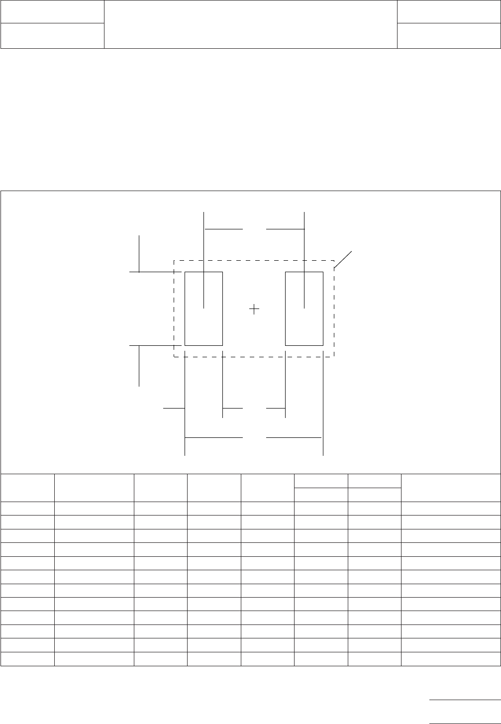
5.0 LAND PATTERN DIMENSIONS
Figure 3 provides the land pattern dimensions for inductors.
These numbers represent industry consensus on the best
dimensions based on empirical knowledge of fabricated land
patterns.
In the table, the dimensions shown are at maximum material
condition (MMC). The least mate-rial condition (LMC) should
not exceed the fabrication (F) allowance shown on page 4.
The LMC and the MMC provide the limits for each dimension.
The dotted line in Figure 3 shows the grid placement court-
yard which is the area required to place land patterns and
their respective components in adjacent proximity without
interference or shorting. Numbers in the table represent the
number of grid elements (each element is 0.5 by 0.5 mm) in
accordance with the international grid detailed in IEC publica-
tion 97.
RLP No.
Component
Identifier (mm) Z (mm) G (mm) X (mm)
C (mm) Y (mm)
Placement Grid
(No. Grid Elements)ref ref
160 2012 Chip 3.00 1.00 1.00 2.00 1.00 4x8
161 3216 Chip 4.20 1.80 1.60 3.00 1.20 6x10
162 4516 Chip 5.80 2.60 1.00 4.20 1.60 4x12
163 2825 Prec 3.80 1.00 2.40 2.40 1.40 6x10
164 3225 Prec 4.60 1.00 2.00 2.80 1.80 6x10
165 4532 Prec 5.80 2.20 3.60 4.00 1.80 8x14
166 5038 Prec 5.80 3.00 2.80 4.40 1.40 8x14
167 3225/3230 Molded 4.40 1.20 2.20 2.80 1.60 6x10
168 4035 Molded 5.40 1.00 1.40 3.20 2.20 8x12
169 4532 Molded 5.80 1.80 2.40 3.80 2.00 8x14
170 5650 Molded 6.80 3.20 4.00 5.00 1.80 12x16
171 8530 Molded 9.80 5.00 1.40 7.40 2.40 8x22
Figure 3 Inductor land pattern dimensions
▼
▼
▼
▼
▼
▼
▼
▼
▼
C
G
Z
X
Y
Grid
placement
courtyard
▼
IPC-782-8-3-3
IPC-SM-782
Subject
Inductors
Date
8/93
Section
8.3
Revision
Page3of4
电子技术应用 www.ChinaAET.com
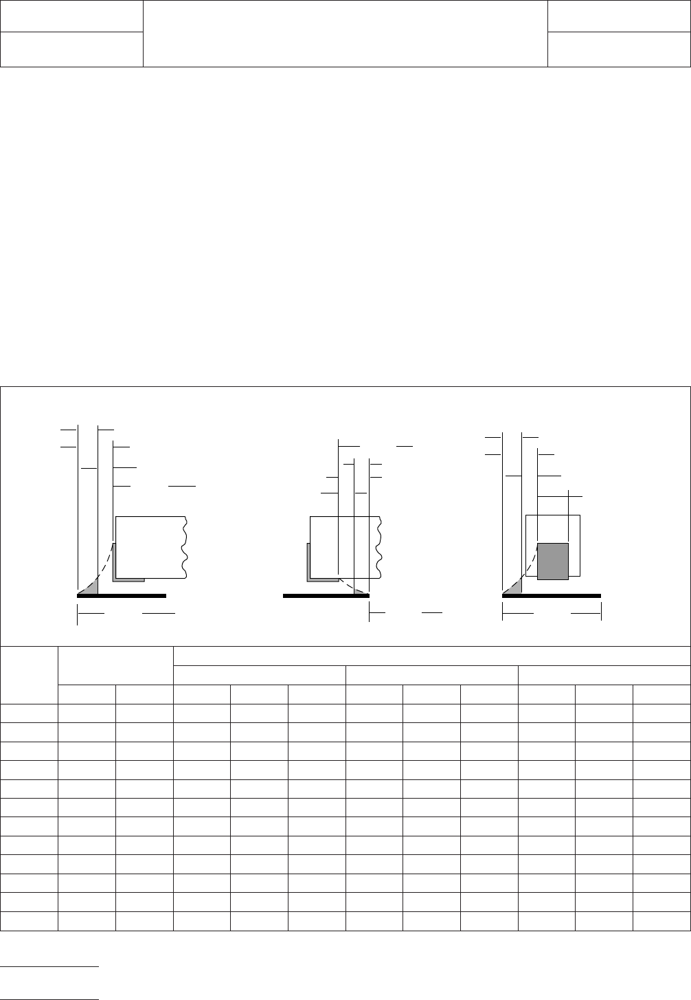
6.0 TOLERANCE AND SOLDER JOINT ANALYSIS
Figure 4 provides an analysis of tolerance assumptions and
resultant solder joints based on the land pattern dimensions
shown in Figure 3. Tolerances for the component dimensions,
the land pattern dimensions (fabrication tolerances on the
interconnecting substrate), and the component placement
equipment accuracy are all taken into consideration.
Figure 4 provides the solder joint minimums for toe, heel, and
side fillets, as discussed in Section 3.3. The tolerances are
addressed in a statistical mode, and assume even distribution
of the tolerances for component, fabrication, and placement
accuracy.
Individual tolerances for fabrication (‘‘F’’) and component
placement equipment accuracy (‘‘P’’) are assumed to be as
given in the table. These numbers may be modified based on
user equipment capability or fabrication criteria. Component
tolerance ranges (C
L
,C
S
, and C
W
) are derived by subtracting
minimum from maximum dimensions given in Figure 2. The
user may also modify these numbers, based on experience
with their suppliers. Modification of tolerances may result in
alternate land patterns (patterns with dimensions other than
the IPC registered land pattern dimensions).
The dimensions for minimum solder fillets at the toe, heel, or
side (J
T
,J
H
,J
S
) have been determined based on industry
empirical knowledge and reliability testing. Solder joint
strength is greatly determined by solder volume. An observ-
able solder fillet is necessary for evidence of proper wetting.
Thus, the values in the table usually provide for a positive sol-
der fillet. Nevertheless, the user may increase or decrease the
minimum value based on process capability.
RLP No.
Tolerance
Assumptions (mm)
Solder Joint
Toe (mm) Heel (mm) Side (mm)
FPC
L
J
T
min J
T
max C
S
J
H
min J
H
max C
WI
J
S
min J
S
max
160 0.2 0.2 0.663 0.32 0.98 0.721 0.02 0.74 0.663 –0.13 0.53
161 0.2 0.2 0.663 0.32 0.98 0.787 0.02 0.81 0.663 –0.18 0.48
162 0.2 0.2 0.663 0.47 1.13 0.970 –0.02 0.95 0.663 –0.13 0.53
163 0.2 0.2 0.663 0.47 1.13 0.773 –0.08 0.70 0.325 0.06 0.39
164 0.2 0.2 0.663 0.52 1.18 0.970 –0.07 0.90 0.490 0.06 0.54
165 0.2 0.2 0.663 0.47 1.13 0.970 –0.02 0.95 0.490 0.05 0.54
166 0.2 0.2 0.663 0.39 1.06 0.758 –0.12 0.64 0.325 0.01 0.33
167 0.2 0.2 0.490 0.46 0.94 0.648 0.17 0.82 0.346 0.03 0.37
168 0.2 0.2 0.583 0.50 1.09 0.837 –0.12 0.72 0.412 –0.11 0.31
169 0.2 0.2 0.663 0.47 1.13 0.894 0.23 1.12 0.346 0.03 0.37
170 0.2 0.2 0.346 0.58 0.92 1.058 0.03 1.09 0.490 –0.14 0.34
171 0.2 0.2 0.583 0.48 1.07 0.837 0.10 0.94 0.412 –0.11 0.31
Figure 4 Tolerance and solder joint analysis
▼
Wmin
Lmin
▼
▼
Zmax
▼
▼
1
/2 T
T
J
T
min
Smax
J
H
min
Xmax
▼
▼
Toe Fillet
1
/2 T
S
▼
▼
▼
Heel Fillet Side Fillet
▼
▼
▼
▼
▼
J
T
max
J
H
max
J
S
max
J
S
min
▼
▼
▼
▼
▼
▼
▼
▼
▼
▼
▼
▼
▼
▼
Gmin
▼
▼
1
/2 T
H
▼
▼
▼
IPC-872-8-3-4
IPC-SM-782
Subject
Inductors
Date
8/93
Section
8.3
Revision
Page4of4
电子技术应用 www.ChinaAET.com