00191413-01.pdf - 第244页
8 Product / PCB User Manual Line Computer UNIX 8.1 PCB Editor Software Version 501.xx 01/99 Issue 8 - 6 8.1.2 Start ing t he PCB Ed itor - In the "program ming mode" the PCB Editor is act ivated by clicki ng on…
User Manual Line Computer UNIX 8 Product / PCB
Software Version 501.xx 01/99 Issue 8.1 PCB Editor
8 - 5
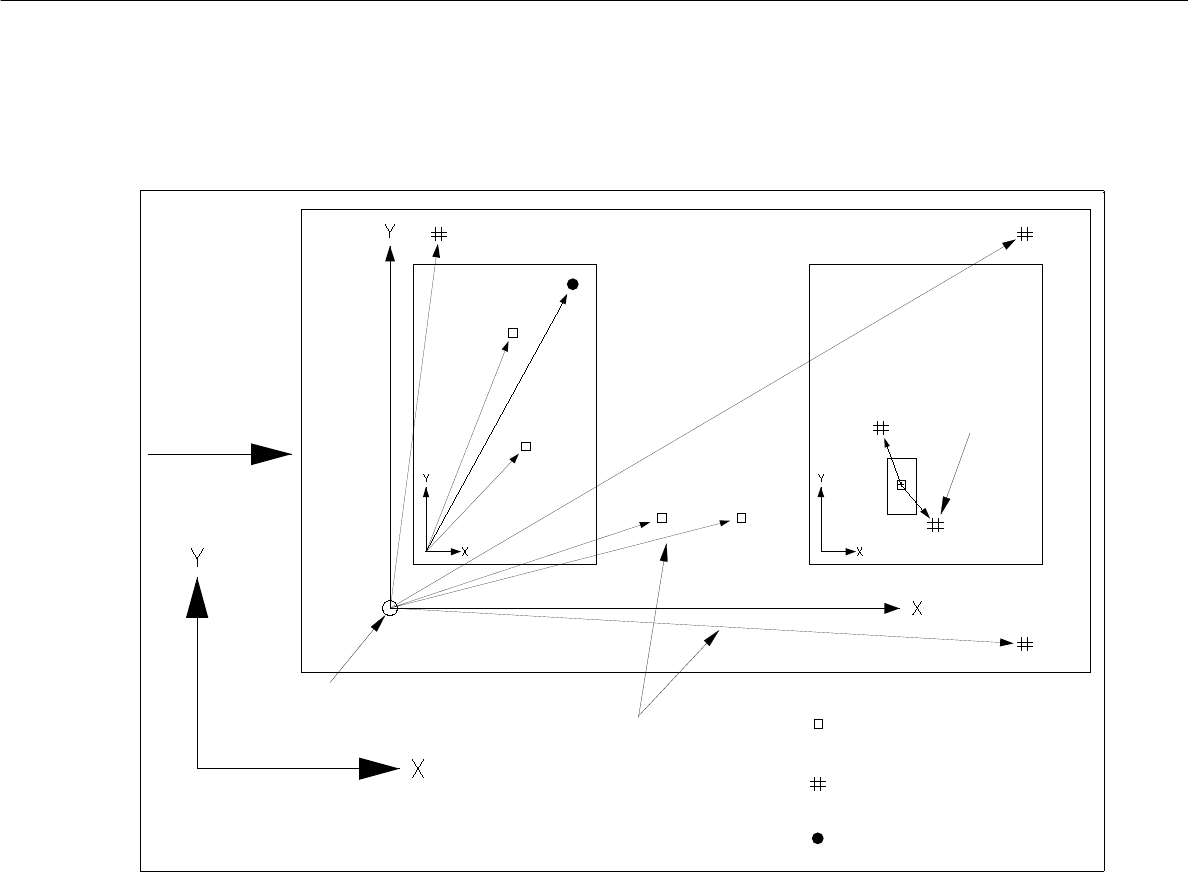
Fig. 8.1.3 Example "Coordinates for Placements Positions, Fiducials, Ink Spots"
placement position
fiducial (PM)
ink dot
vectors
PCB transport-
machine’s coordinate system
fiducial for
placem. pos.
PCB zero point
direction
recognition
8 Product / PCB User Manual Line Computer UNIX
8.1 PCB Editor Software Version 501.xx 01/99 Issue
8 - 6
8.1.2 Starting the PCB Editor
- In the "programming mode" the PCB Editor is activated by clicking on the PCB icon on the desktop or
via the Data Manager (see chapt. 4).
- If the LC program was installed for the "control mode", the PCB Editor can be started via the
"PRODUCT" menu on the desktop, or via the Data Manager.
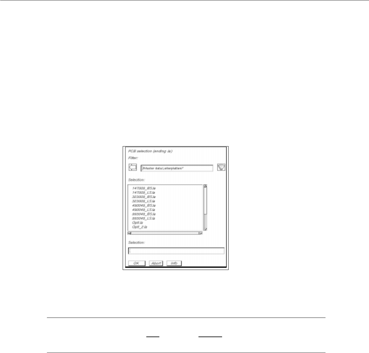
● Click on the PCB icon on the desktop (or the "PCB Editor" option on the "PRODUCT" menu).
The FSB containing the files of all already-defined PCBs is opened.
● Select name "xxx.la" of the PCB desired by double-clicking, or enter the new number using the
keyboard and confirm with OK.
The main window of the PCB Editor, the so-called Structure Editor (see Fig. 8.1.4), is opened.
NOTE
The name of the PCB may comprise max.
20 characters including the suffix ".la". Some characters
must not be used for the name, see chapt. 2, section 2.3 in this connection.
User Manual Line Computer UNIX 8 Product / PCB
Software Version 501.xx 01/99 Issue 8.1 PCB Editor
8 - 7
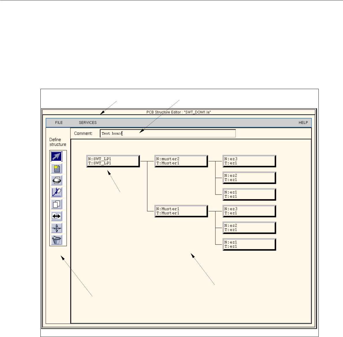
8.1.3 Main Display Window of Structure Editor
In the following, the sections of the main display window and their functions are described.
Fig. 8.1.4 Main window "PCB Structure Editor" (Display Structure Mode)
The main display window is subdivided as follows:
- Menu
- Editing field
- Display Area
- Command Area (only available in the structure mode)
- Setting Area (only available in the graphic mode, Fig. 8.1.6)
menu bar
display area
command area
uppermost partial
PCB structure
editing field