00191413-01.pdf - 第254页
8 Product / PCB User Manual Line Computer UNIX 8.1 PCB Editor Software Version 501.xx 01/99 Issue 8 - 16 8.1.3.4 Setting Area of Structure E ditor (Graphic Mode) - For a better visu alizatio n of the PCB in th e displa y…
User Manual Line Computer UNIX 8 Product / PCB
Software Version 501.xx 01/99 Issue 8.1 PCB Editor
8 - 15
- Moving a partial PCB structure with corresponding PCB type
This command serves to move a partial PCB structure, together with a cross-reference to a PCB type,
within a given PCB structure.
● Activate icon .
● Select target PCB type where partial PCB structure is to be moved to.
● Select source PCB type containing the partial PCB structure to be moved.
The partial PCB structure - appended to the target PCB type - is shown in the display area.
- Deleting a partial PCB structure
● Activate icon .
● Select PCB structure with a mouse-click.
The partial PCB structure is deleted (without confirmation!).
CAUTION
"Delete" is to be deactivated by selecting another command, as otherwise all other PCB types that are
subsequently clicked on will also be deleted.
8 Product / PCB User Manual Line Computer UNIX
8.1 PCB Editor Software Version 501.xx 01/99 Issue
8 - 16
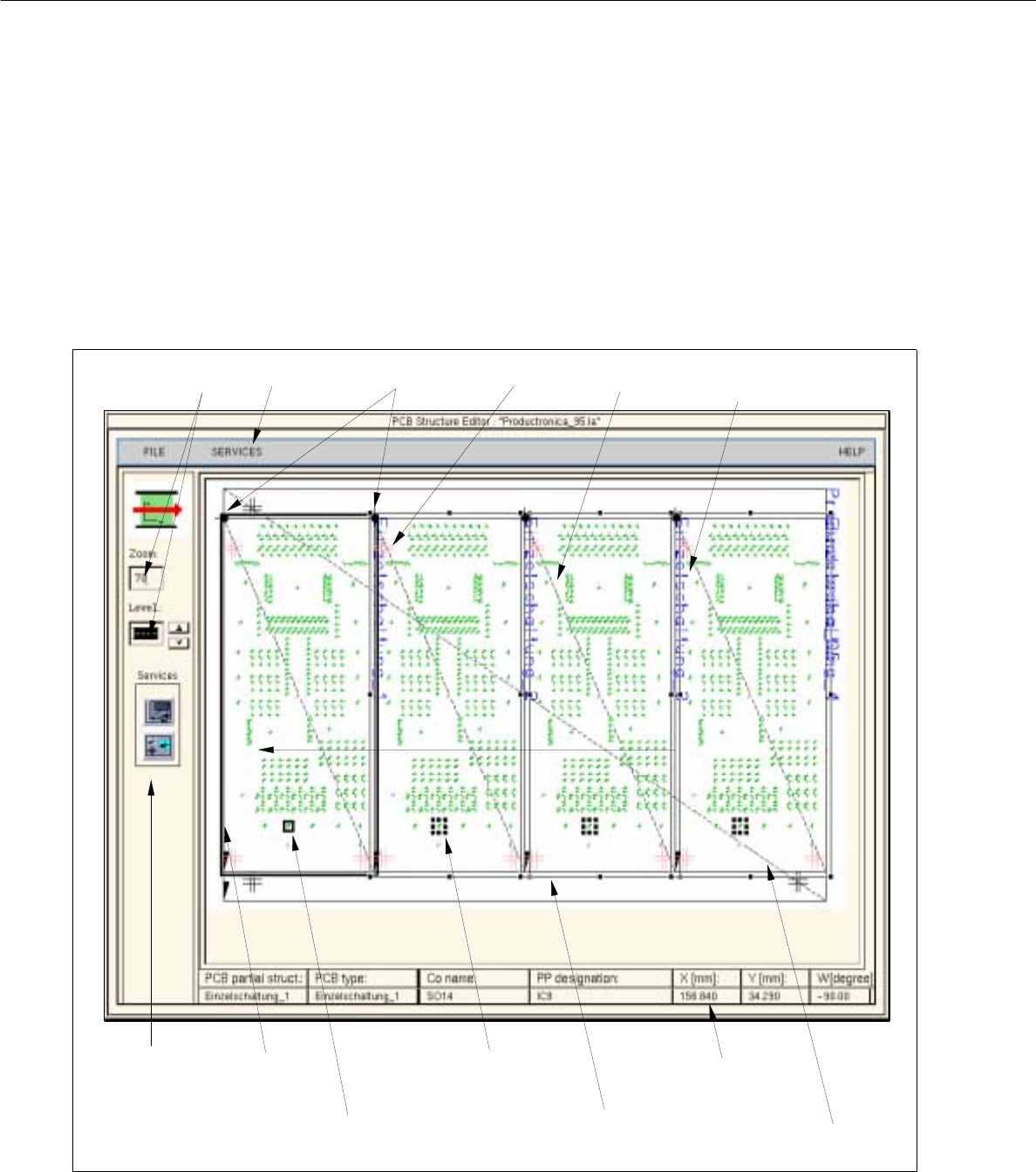
8.1.3.4 Setting Area of Structure Editor (Graphic Mode)
- For a better visualization of the PCB in the display area, a zoom factor (10 - 999%) can be entered in the
editing field of the setting area, with the factor "100" corresponding to reality.
- The remaining display options are symbolized by icons (see Fig. 8.1.6). The desired setting can be achie-
ved by activating an icon (see the description below).
Fig. 8.1.6 Main Window "Structure Editor" ("Graphic Mode" Display)
PCB
dimensional vector
setting area
menu bar name of the PCB
substructure
selected placement
position (PP)
offset vector
PCB zero points
editing fields
fiducial
x-axis (+)
outline (dimensions)
of the PCB
data of the selected
placement position
placement pos.
linked to the selected
placement pos.
User Manual Line Computer UNIX 8 Product / PCB
Software Version 501.xx 01/99 Issue 8.1 PCB Editor
8 - 17
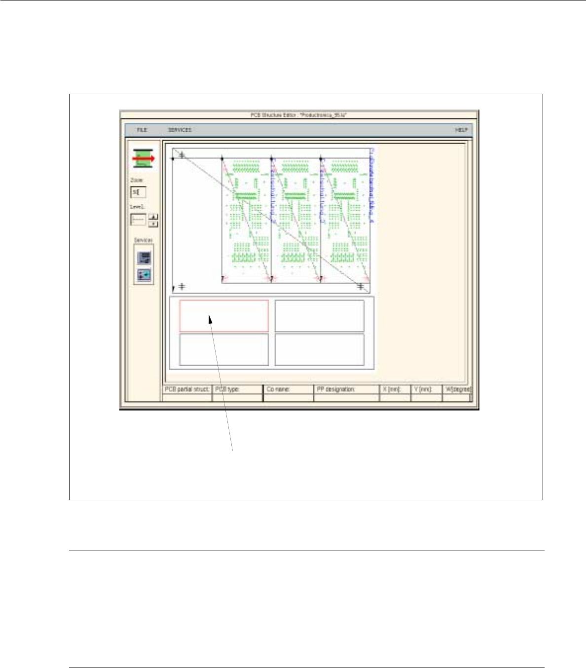
Fig. 8.1.7 "Graphic Mode" display with additional structure graphic
NOTE pertaining to Fig. 8.1.7
The Structure Graphic symbolically represents the overall structure of the PCB and is only created for those
PCBs with at least one substructure whose offset values are not completely defined. The Structure Graphic
does not provide any geometrical information about the substructure, but rather merely reveals the interrelation-
ships of the substructures as well as the status of the offset data of the substructures. In the Structure Graphic
the substructures are represented as rectangles of different colors.
The meaning of the colors is described in section 8.1.3.7.
Structure Graphic
(is only displayed if the offset values are not completely defined)