00191413-01.pdf - 第267页
User Manual Line Computer UNIX 8 Product / PCB Software Version 501.xx 01/99 Issue 8.1 PCB Editor 8 - 29 - Max. comp. height tol. (copl.): [ 1/1000 mm] This entr y is onl y requi red for coplanar ity measure ment. The ma…
8 Product / PCB User Manual Line Computer UNIX
8.1 PCB Editor Software Version 501.xx 01/99 Issue
8 - 28
8.1.4.2 SERVICES Menu
- Opening the Placement Position Editor
● Click on SERVICES --> Placement Position Editor.
The window of the Placement Position Editor is opened (see section 8.1.6).
8.1.4.3 Editing Area of Cluster Editor
INPUT POSSIBILITIES
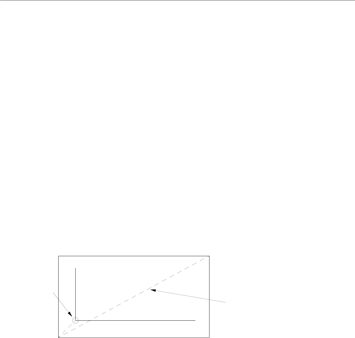
The outer measurements of the current PCB type (cluster) are defined by the dimensional values in x and
y-directions. Values up to max. 999.999 can be entered in each case.
- Vector (0,0)-->corner_1 X [mm] or Y [mm]
example: X = -10.000; Y = -10.000
- Vector corner_1-->corner_2 X [mm] or Y [mm]
example: X = 80.000; Y = 50.000
- PCB height: h [mm]
In this field the PCB thickness is to be entered; it is possible to
enter a number with three places before and after the decimal
point.
+ Y
+ X
corner 1
corner 2
vector
0, 0

User Manual Line Computer UNIX 8 Product / PCB
Software Version 501.xx 01/99 Issue 8.1 PCB Editor
8 - 29
- Max. comp. height tol. (copl.): [1/1000 mm]
This entry is only required for coplanarity measurement.
The max. component height tolerance is to be entered;
values up to max. 999 can be entered.
8.1.4.4 Setting Area Cluster Editor
ENTRIES REQUIRED for the Placement Procedure
- Place. position recognition: yes / no
If fiducials for placement position recognition have been
defined, "Place.position recognition" can be turned on or
off for the current PCB type (cluster) by selecting "yes" or
"no", respectively.
- Ink spot: yes / no
"Ink spot recognition" can be turned on or off for the
current PCB type (cluster) by selecting "yes" or "no",
respectively.
- PCB position recognition: yes / no
"PCB position recognition can be turned on or off for the
current PCB type (cluster) by selecting "yes" or "no",
respectively.
- Omit cluster: omit
If this setting has been activated, the current PCB type
(cluster) will be skipped during placement when the
complete PCB is processed.
Procedure to be followed for editing:
- Editing the cluster data
● Position the mouse cursor in the editing field and make entries using the keyboard.
- Copying individual entries using the mouse from/into editing fields of the Cluster Editor in the same
window or into another open window of the Cluster Editor
● Hold down the left mouse button and move the mouse cursor over the entries to be copied
(exactly to the end of the last character) and then release the mouse button.
The lines concerned now darken.
● Hold down the center mouse button and position the cursor in the respective editing field of the
window of the Cluster Editor where the entries are to be inserted and then release the mouse
button. The copied entries are now displayed.
8 Product / PCB User Manual Line Computer UNIX
8.1 PCB Editor Software Version 501.xx 01/99 Issue
8 - 30
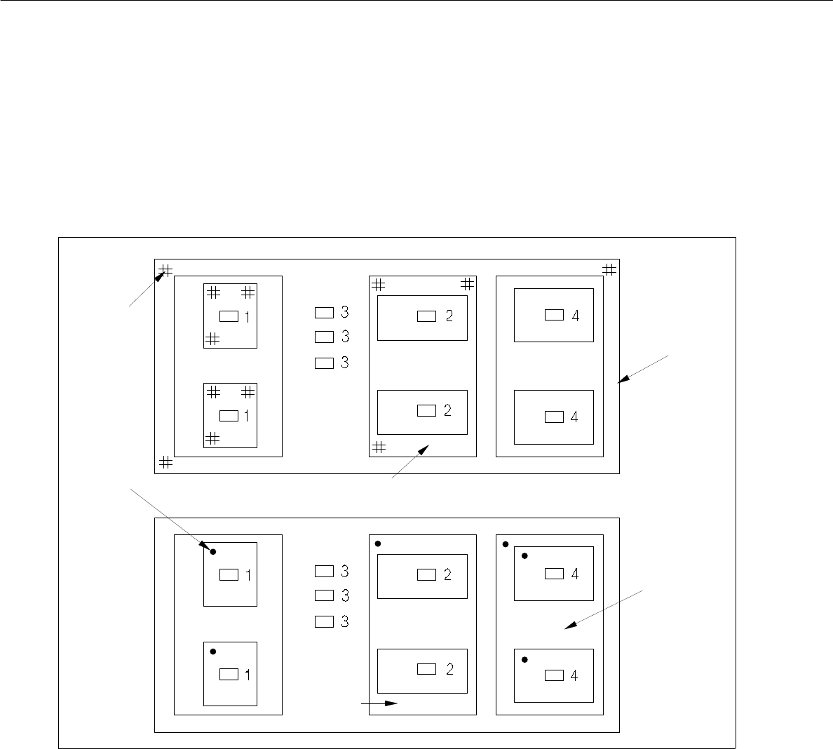
8.1.5 Fiducial Editor Window
With the aid of the menu and the input fields of the Fiducial Editor the fiducials (for PCB position recognition)
and ink spots (to identify faulty clusters) required for a specific PCB type can be set or deselected.
Examples of allocations of fiducials and ink spots are shown and described in the following.
Fig. 8.1.9 Allocation of Fiducial Sets for Position Recognition and Allocation of Ink Spots (example)
Fiducial set for position recognition:
Fiducial set of the single circuit applies to component 1.
Fiducial set of group 2 applies to components 2.
Fiducial set of group 1 applies to components 3.
Fiducial set of group 1 applies to components 4.
Ink Spots:
The ink spot of the single circuit applies to components 1.
The ink spot of group 2 applies to components 2.
No ink spot applies to components 3.
The ink spot of group 3 applies to components 3.
group 1
group 2
group 3
group 2
fiducial
ink dot