00191413-01.pdf - 第560页
17.3 Description of Components and PCBs User Manual Line Computer UNIX 17.3.2 PCB 2: Focus on Packa g e Form Description Software Vers ion 501.xx 01/99 Issue 17 - 28 Package fo rm description for pa ckage form 1503 conti…

User Manual Line Computer UNIX 17.3 Description of Components and PCBs
Software Version 501.xx 01/99 Issue 17.3.2 PCB 2: Focus on Packa
g
e Form Description
17 - 27
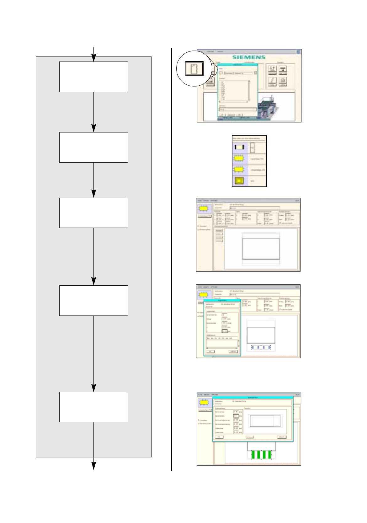
To define the pin model for package form 1502, proceed as follows:
38. Select one of the two pin
g
roups b
y
clickin
g
on it.
39. Click on the
Pin/Ball
button.
The Pin model data window is opened.
40. Enter the pin model data,
confirm b
y
pressin
g
the Enter ke
y
, here:see chart:
The automaticall
y
calculated values of the other editin
g
fields can be adopted.
Ever
y
time the Enter ke
y
is pressed, the displa
y
of the pin model is updated.
41. Click on the
OK
button.
The Pin model data window is closed. The packa
g
e form with pins is displa
y
ed.
To enter the handling data for package form 1502, proceed as follows:
42. Activate the
Handling data
button.
The screen for enterin
g
the handlin
g
data is displa
y
ed.
43. Activate the
Nozzle
button in the command area.
44. Click on the
Create
button.
The Nozzle t
y
pe selection window containin
g
a list of the nozzle t
y
pes is loaded.
45. Click on a nozzle, here:
416
.
The selection window closes, the nozzle is transferred to the view area.
46. Activate the
Sensor type
button.
47. Click on the
Create
button.
The Sensor t
y
pe selection window containin
g
a list of the sensor t
y
pes is opened.
48. Click on a sensor t
y
pe, here:
7
.
The selection window closes, the sensor t
y
pe is transferred to the view area.
49. In the ’Handlin
g
values’ editin
g
area, enter the applicable value in the
Placement force
field, here:
2
.
50. In the ’Centerin
g
’ selection box, activate the applicable buttons, here:
External centering
.
51. In this example, the preselected settin
g
s for the handlin
g
values, the handlin
g
instructions and the ’Acce-
leration’ special handlin
g
option can be accepted as the
y
are. No chan
g
es are re
q
uired.
52. Click on the
Save
option on the
FILE
menu.
The data are now saved.
To allocate a feeder to package form 1502:
53. Click on the
Starting Feeder Editor
option on the
SERVICES
menu.
The Feeder Editor is opened.
54. Activate the
Allocate
icon .
55. Activate a button for the line or a feeder part, here:
Line
.
The entire line is hi
g
hli
g
hted in li
g
ht-
g
reen.
56. Click on the appropriate feeder on the list of placeable feeders, here:
FD~S_G_32_III
.
The feeder is transferred to the Feeder selection field.
57. In the Feeder Editor click on the
Save
option on the
FILE
menu.
The data are now saved.
58. Click on the
Quit
option on the
FILE
menu.
The Feeder Editor is closed.
59. In the Packa
g
e Form Editor click on the
Quit
option on the
FILE
menu.
The Packa
g
e Form Editor is closed.
Pin length L
1
Pin width b
0.8 0.2
17.3 Description of Components and PCBs User Manual Line Computer UNIX
17.3.2 PCB 2: Focus on Packa
g
e Form Description Software Version 501.xx 01/99 Issue
17 - 28
Package form description for package form 1503
continued from pa
g
e 17-26
continued on pa
g
e 17-30
Defining pin model
Entering dimensions
Defining package
form type for package
form 1503
Creating pin group
Opening Package
Form Editor for
package form 1503
User Manual Line Computer UNIX 17.3 Description of Components and PCBs
Software Version 501.xx 01/99 Issue 17.3.2 PCB 2: Focus on Packa
g
e Form Description
17 - 29
C) Description of an irregular FDC using package form 1503 as an example
To open the Package Form Editor for package form 1503, proceed as follows:
60. On the desktop click on the icon of the Packa
g
e Form Editor .
The file selection window is opened.
61. Click on the
Selection
editin
g
field.
62. Enter the packa
g
e form number, here:
1503.gf
and click on the
OK
button.
The Packa
g
e Form Editor with the Packa
g
e form t
y
pe selection window is opened.
To define the package form type „irregular FDC“ for package form 1503, proceed as follows:
63. Click on the
Irregular FDC
t
y
pe in the Packa
g
e form t
y
pe selection window.
The selection window is closed.
64. In the Packa
g
e Form Editor click on the
Comment
editin
g
field, enter a uni
q
ue comment, here:
Micro-X
.
To enter the dimensions for package form 1503, proceed as follows:
65. Enter the dimensions of the packa
g
e form with pins in the Nominal dimensions editin
g
area, confirm
y
our
entr
y
b
y
pressin
g
the Enter ke
y
, here: see chart:
The tolerances are entered automaticall
y
.
The packa
g
e form with the tolerance ran
g
e is displa
y
ed.
66. Enter the dimensions of the packa
g
e form without pins in the Bod
y
editin
g
area, confirm b
y
pressin
g
the
Enter ke
y
, here: see chart:
(
These entries are onl
y
re
q
uired for the displa
y
)
.
The displa
y
of the packa
g
e form is updated.
67. In this example the default values of the Packa
g
in
g
tolerances and Features editin
g
areas can be
adopted, no entries are re
q
uired.
To create the lower pin group (pins 1 to 4) of package form 1503, proceed as follows:
68. Click on the
Create
button.
The Group data window is opened. On the upper side of the component a predefined pin
g
roup with three
pins
(
g
ra
y
areas
)
is displa
y
ed.
69. Overwrite the default values in the editin
g
fields with the pin
g
roup data for packa
g
e form 1503
(
see dis-
pla
y
s in On-line Help
)
and confirm
y
our entr
y
b
y
pressin
g
Enter ke
y
, here: see chart:
Ever
y
time the Enter ke
y
is pressed, the displa
y
of the pin
g
roup
(g
ra
y
areas
)
is updated, the pin
g
roups
are now displa
y
ed on the bottom side of the component.
70. Click on the
OK
button.
The Group data window is closed.
To define the pin model for the lower pin group of package form 1503, proceed as follows:
71. Select one of the two pin
g
roups b
y
clickin
g
on it.
72. Click on the
Pin/Ball
button.
The Pin model data window is opened.
73. Enter the pin model data, here: see chart:
In this example the automaticall
y
calculated values of the other editin
g
fields can be adopted. Ever
y
time
the Enter ke
y
is pressed, the displa
y
of the pin model is updated.
74. Click on the
OK
button.
The Pin model data window is closed. The packa
g
e form to
g
ether with the pins is displa
y
ed at the
bottom side.
X
(Length D)
Y
(Width H
E
)
Z
(Height A)
6.5 7 1.8
X
(Length D)
Y
(Width E)
6.5 3.5
No. of pins
Spacing
e2
Pin angle
X (BG
Off
) Y (BG
Off
)
4 1.27 -90 0 -2.625
Pin length BL Pin width b
1.75 0.6