00191413-01.pdf - 第572页
17.3 Description of Components and PCBs User Manual Line Computer UNIX 17.3.2 PCB 2: Focus on Packa g e Form Description Software Vers ion 501.xx 01/99 Issue 17 - 40 Fig. 17.3.6 Placement Position Editor for PCB 2 Enter …
User Manual Line Computer UNIX 17.3 Description of Components and PCBs
Software Version 501.xx 01/99 Issue 17.3.2 PCB 2: Focus on Packa
g
e Form Description
17 - 39
To define the ink spot, proceed as follows:
140.In the Fiducial Editor activate the
Insert
button.
141.Click on the
Fiducial set name
editin
g
field.
142.Enter a name for the new fiducial set
(
ink spot
)
, here:
ink
.
143.Click on the
Accept fiducial set
button.
The ink fiducial set appears on the fiducial list.
144.Click on the ink fiducial set on the fiducial list.
145.Click on the
Fiducial
editin
g
field.
146.Enter the fiducial number, here:
48
.
147.Click on the individual editin
g
fields for the coordinetes and enter
the coordinates
(
do not confirm with the Enter ke
y)
, here: see chart:
148.Click on the
Accept fiducial data
button.
The data of the ink spot are transferred to the list of the fiducials of the fiducial set.
149.Activate the
Ink spot fiducial set
button.
150.Click on the ink fiducial set on the fiducial list.
The ink fiducial set name is preceded b
y
an
I
for ink spot.
151.Click on the
Quit
option on the
FILE
menu.
The Fiducial Editor is closed.
152.In the Cluster Editor click on the
Quit
option on the
FILE
menu.
The Cluster Editor is closed.
To create clusters and single circuits, proceed as follows:
no clusters and sin
g
le circuits are present.
To enter the placement positions, proceed as follows:
153.In the Component Editor activate the Select icon .
154.Click on the PCB
(
rectan
g
le
)
.
The rectan
g
le is hi
g
hli
g
hted in
g
reen.
155.Click on the
Placement Position Editor
option on the
SERVICES
menu.
The Placement Position Editor is opened.
156.Position the cursor in the entr
y
field and enter the placement positions in accordance with Tab. 17.3-3 on
pa
g
e 17-20. The individual entries are to be separated b
y
a blank. Ever
y
line is to be confirmed b
y
pres-
sin
g
the Enter ke
y
. See also Fi
g
. 17.3.6 on pa
g
e 17-40.
157.When the entr
y
has been completed, activate the Check icon .
The values entered are checked and arran
g
ed in columns.
158.Click on the
Quit
option on the
FILE
option.
The Placement Position Editor is closed.
To save the PCB data, proceed as follows:
159.In the PCB Editor click on the
Save
option on the
FILE
menu.
The PCB data are saved.
160.Click on the
Quit
option on the
FILE
menu.
The PCB Editor is closed. The description of PCB 2 is terminated.
Fiducial number X Y
48 15 0
17.3 Description of Components and PCBs User Manual Line Computer UNIX
17.3.2 PCB 2: Focus on Packa
g
e Form Description Software Version 501.xx 01/99 Issue
17 - 40
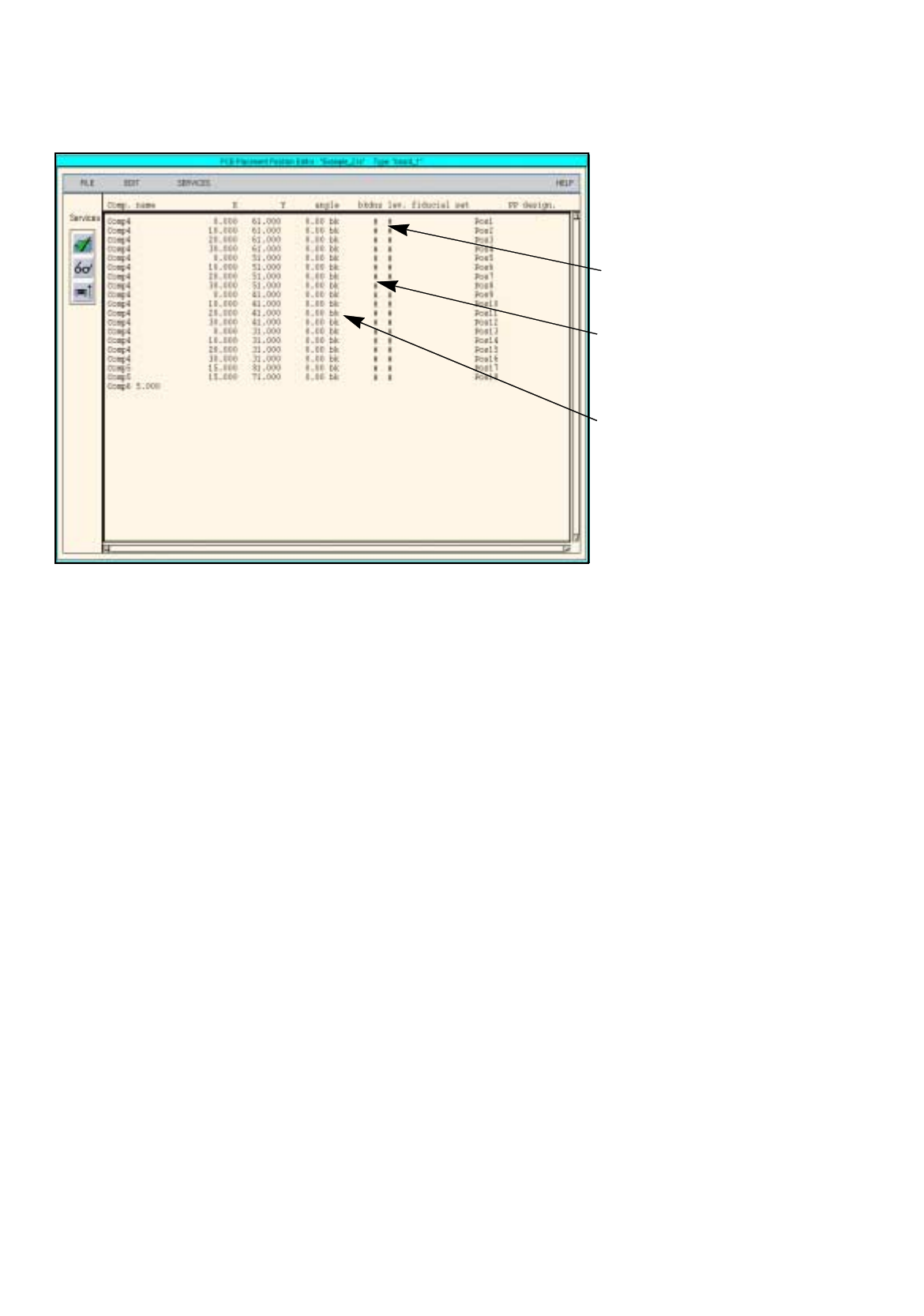
Fig. 17.3.6 Placement Position Editor for PCB 2
Enter fiducial set name
# = no fiducials defined for the
placement position
b = placin
g
k =
g
luein
g
d = dispensin
g
(
solder paste
)
n = reworkin
g
s = blockin
g
(
from placement
)
Enter number of placement
level
# = no level defined for the pla-
cement position
User Manual Line Computer UNIX 17.3 Description of Components and PCBs
Software Version 501.xx 01/99 Issue 17.3.3 PCB 3: Focus on Cluster Technique
17 - 41
pattern_2
pattern_1
pattern_3
pattern_4
board 1
board2
board 3
board 1
board2
board 3
board 3
board2
board 1
board 3
board2
board 1
Example_3
5
10
15
Corner
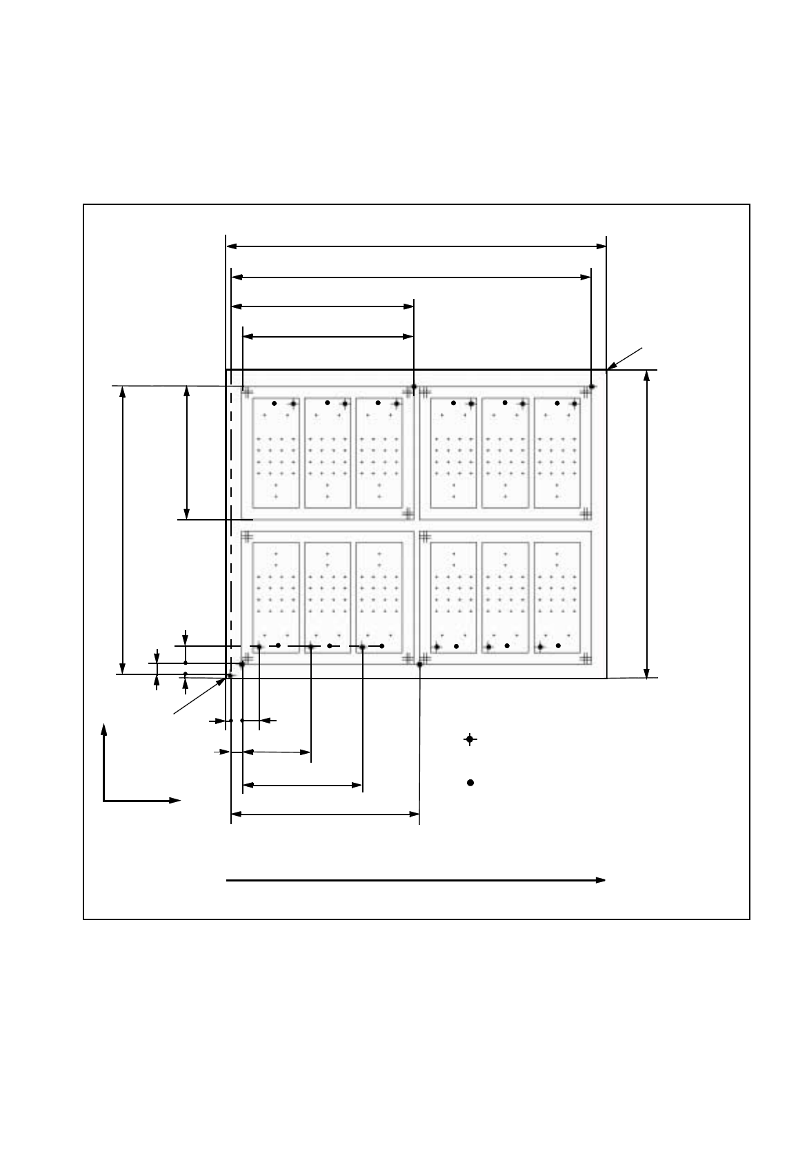
17.3.3 PCB 3: Focus on Cluster Technique
PCB 3 consists of four clusters
(
pattern
)
each of which comprises three sin
g
le circuits
(
board
)
. The dimensions
and the placement confi
g
uration of the sin
g
le circuits corresponds to those of PCB 2. Clusters 3 and 4 are ro-
tated b
y
180°. For each cluster a PCB position reco
g
nition operation is performed. Three fiducials are available
in each case. An ink spot is located on each sin
g
le circuit.
335
272
5
X
Y
PCB coordinate
system 0°
Direction of travel
150
116
10
15
60
105
165
Corner
PCB hei
g
ht= 1.5 mm
Zero point of the different levels:
PCB, cluster, sin
g
le circuit
Ink spot
Fig. 17.3.7 Dimensions PCB 3
252
160
315