00191413-01.pdf - 第578页
17.3 Description of Components and PCBs User Manual Line Computer UNIX 17.3.3 PCB 3: Focus on Cluster Technique Software Version 501.xx 01/99 Issue 17 - 46 No ink spot i s present . Loading cluster data and plac ement po…
User Manual Line Computer UNIX 17.3 Description of Components and PCBs
Software Version 501.xx 01/99 Issue 17.3.3 PCB 3: Focus on Cluster Technique
17 - 45
To create a cluster on the PCB, create as follows:
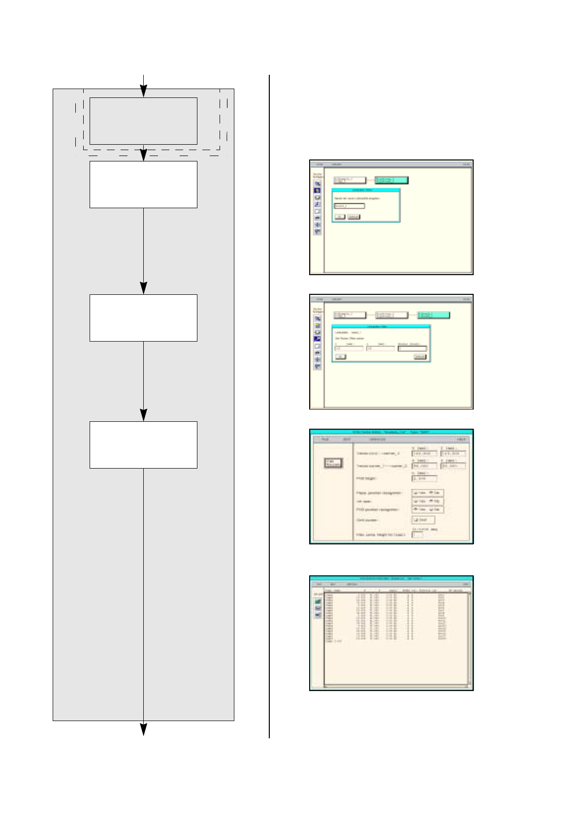
15. In the PCB Editor, activate the Create icon .
16. Click on the PCB, here:
Example_3
.
A dialo
g
box is opened.
17. Click on the editin
g
field.
18. Enter the name of the cluster, here:
pattern_1,
and click on the
OK
button.
The dialo
g
box is closed. The new cluster is displa
y
ed at the second level.
To enter the cluster offset values, proceed as follows:
19. Activate the Coordinate s
y
stem icon .
20. Click on the cluster, here:
pattern_1
.
A dialo
g
box is opened.
21. Click on the individual editin
g
fields and enter the offset values, see Fi
g
. 17.3.7 on pa
g
e 17-41.
22. Click on the
OK
button.
The dialo
g
box is closed.
To enter the dimensions of the cluster, proceed as follows:
23. Activate the Select icon .
24. Click on the cluster, here:
pattern_1
.
25. Click on the
Cluster Editor
option on the
SERVICES
menu.
The Cluster Editor is opened.
26. Enter the dimensions of the cluster, see Fi
g
. 17.3.7 on pa
g
e 17-41.
To define the fiducials for the cluster, proceed as follows:
27. In the Cluster Editor click on the
Edit fiducials
button.
The Fiducial Editor is opened.
28. Activate the
Insert
button.
29. Click on the
Fiducial set name
editin
g
field.
30. Enter a name for the new fiducial set, here:
Set_1
.
31. Click on the
Accept fiducial set
button.
The fiducial set Set_1
appears on the fiducial list.
32. Click on the fiducial set Set_1
on the fiducial list.
33. Click on the
Fiducial
editin
g
field.
34. Enter the fiducial number for the first fiducial, here:
48
.
35. Click on the individual editin
g
fields for the coordinates, enter
coordinates do not confirm with the Enter ke
y)
, here: see chart:
36. Click on the
Accept fiducial data
button.
The data of the fiducial are transferred to the list of the fiducials of the fiducial set.
37. Define the remainin
g
fiducials analo
g
ousl
y
, here:
fiducials
48
and
48
.
38. Activate the
PCB position recognition
button.
39. Click on the fiducial set Set_1 on the fiducial list.
The fiducial set name Set_1
is preceded b
y
an
L
for the PCB position reco
g
nition.
40. Click on the
Quit
option on the
FILE
menu.
The Fiducial Editor is closed.
41. Click on the
Quit
option on the
FILE
menu.
The Cluster Editor is closed.
Ficucial number X Y
48 5 5
48 5 111
48 145 5
17.3 Description of Components and PCBs User Manual Line Computer UNIX
17.3.3 PCB 3: Focus on Cluster Technique Software Version 501.xx 01/99 Issue
17 - 46
No ink spot is present.
Loading cluster data
and placement
positions
continued from pa
g
e 17-44
Creating a single
circuit
continued on pa
g
e 17-48
Entering offset values
for the single circuit
PCB description
Defining ink spot

User Manual Line Computer UNIX 17.3 Description of Components and PCBs
Software Version 501.xx 01/99 Issue 17.3.3 PCB 3: Focus on Cluster Technique
17 - 47
Defining ink spot:
no ink spot is present.
To create a single circuit in a cluster, proceed as follows:
42. Activate the Create icon .
43. Click on the cluster, here:
pattern_1
.
A dialo
g
box is opened.
44. Click on the editin
g
field.
45. Enter the name for the sin
g
le circuit, here:
board_1,
and click on the
OK
button.
The dialo
g
box is closed. The new sin
g
le circuit is displa
y
ed at the third level.
To enter the offset values for the single circuit, proceed as follows:
46. Activate the Coordinate s
y
stem icon .
47. Click on the sin
g
le circuit, here:
board_1
.
A dialo
g
box is opened.
48. Click on the individual editin
g
fields and enter the offset values, see Fi
g
. 17.3.7 on pa
g
e 17-41.
49. Click on the
OK
button.
The dialo
g
box is closed.
To load the cluster data and placement positions of another PCB for the single circuit:
50. Activate the Select icon .
51. Click on the sin
g
le circuit, here:
board_1
.
52. Click on the
Cluster Editor
option on the
SERVICES
menu.
The Cluster Editor is opened.
53. Click on the
Structure Editor
option on the
SERVICES
menu.
A file selection window is opened.
54. Select a PCB b
y
double-clickin
g
, here:
Example_2.la
.
The PCB Editor for Example_2.la is opened.
55. Click on the PCB
(
rectan
g
le
)
, here:
Example_2
.
56. Usin
g
the ke
y
combination Alt+Tab chan
g
e to the Cluster Editor of the sin
g
le circuit, here:
board_1
.
57. Click on the
Load cluster data from
option on the
EDIT
menu.
A dialo
g
box containin
g
the name of the source cluster is displa
y
ed.
58. Click on the
OK
button.
The cluster data of the other PCB, here:
Example_2
, are transferred to the current sin
g
le circuit, here:
board_1
, the dialo
g
box is closed. The Placement Position Editor is opened.
59. Usin
g
the ke
y
combination Alt+Tab chan
g
e to the PCB Editor of the other PCB, here:
Example_2.la
.
60. Click on the PCB, here:
Example_2.la
.
61. Usin
g
the ke
y
combination Alt+Tab chan
g
e to the Placement Position Editor of the sin
g
le circuit, here:
board_1
.
62. Click on the
Load placement position from
option on the
EDIT
menu.
A dialo
g
box containin
g
the name of the source cluster is displa
y
ed.
63. Click on the
OK
button.
The placement positions of the other PCB, here:
Example_2
, are transferred to the sin
g
le circuit, here:
board_1
, the dialo
g
box is closed.
64. Click on the
Quit
option on the
FILE
menu.
The Placement Position Editor is closed.