00191413-01.pdf - 第582页
17.3 Description of Components and PCBs User Manual Line Computer UNIX 17.3.3 PCB 3: Focus on Cluster Technique Software Version 501.xx 01/99 Issue 17 - 50 The entr y of plac ement pos itions i s dispense d with for th e…

User Manual Line Computer UNIX 17.3 Description of Components and PCBs
Software Version 501.xx 01/99 Issue 17.3.3 PCB 3: Focus on Cluster Technique
17 - 49
65. In the Cluster Editor activate the appropriate buttons for
PCB position recognition
and
Place. position
recognition
, here: for both options
no
.
66. Activate the appropriate button for
Ink spot
, here:
yes
.
67. Click on the
Quit
option on the
FILE
menu.
The Cluster Editor is closed
To duplicate a single circuit, proceed as follows:
68. Activate the Duplicate icon .
69. Click on the sin
g
le circuit, here:
board_1
.
A dialo
g
box is opened.
70. Click on the editin
g
field.
Enter the name for the new sin
g
le circuit, here:
board_2,
and click on the
OK
button.
The dialo
g
box is closed. The new sin
g
le circuit is displa
y
ed at the third level.
71. Duplicate the other sin
g
le circuit, here:
board_3
, analo
g
ousl
y
.
To enter the offset values for the duplicated single circuits, proceed as follows:
72. Activate the Coordinate s
y
stem icon .
73. Click on a sin
g
le circuit, here:
board_2
.
A dialo
g
box is opened.
74. Click on the individual editin
g
fields and enter the offset values, see Fi
g
. 17.3.7 on pa
g
e 17-41.
75. Click on the
OK
button.
The dialo
g
box is closed.
76. Enter the offset values for the other sin
g
le circuits, here:
board_3
analo
g
ousl
y
.
To duplicate a cluster together with the single circuits contained therein:
77. Activate the Duplicate icon .
78. Click on the cluster
y
ou wish to duplicate, here:
pattern_1
.
A dialo
g
box is opened.
79. Click on the editin
g
field and enter the name, here:
pattern_2
.
80. Click on the
OK
button.
A new cluster with three sin
g
le circuits each is set up. All data of the duplicated cluster are adopted.
81. Duplicate the other clusters, here:
pattern_3
and
pattern_4,
analo
g
ousl
y
.
To enter the offset values for the duplicated clusters, proceed as follows:
82. Activate the Coordinate s
y
stem icon .
83. Click on a duplicated cluster, here:
pattern_2
.
A dialo
g
box is opened.
84. Click on the individual editin
g
fields and enter the offset values, see Fi
g
. 17.3.7 on pa
g
e 17-41.
85. Click on the
OK
button.
The dialo
g
box is closed.
86. Enter the offset values for the other sin
g
le circuits, here:
pattern_3
,
pattern_4
analo
g
ousl
y
.
Defining fiducials:
the definition of the fiducials is dispensed with for the duplicate.
Defining ink spot:
the definition of the ink spot is dispensed with for the duplicate.

17.3 Description of Components and PCBs User Manual Line Computer UNIX
17.3.3 PCB 3: Focus on Cluster Technique Software Version 501.xx 01/99 Issue
17 - 50
The entr
y
of placement positions is dispensed
with for the duplicate.
FILE
Save
FILE
Quit
Entering placement
positions
Saving PCB data
continued from pa
g
e 17-48
User Manual Line Computer UNIX 17.3 Description of Components and PCBs
Software Version 501.xx 01/99 Issue 17.3.3 PCB 3: Focus on Cluster Technique
17 - 51
Entering placement positions:
the entr
y
of placement positions is dispensed with for the duplicate.
To save the PCB data, proceed as follows:
87. In the PCB Editor click on the
Save
option on the
FILE
menu.
The PCB data are saved.
88. Click on the
Quit
option on the
FILE
menu.
The PCB Editor is closed. The description of PCB 3 is completed.
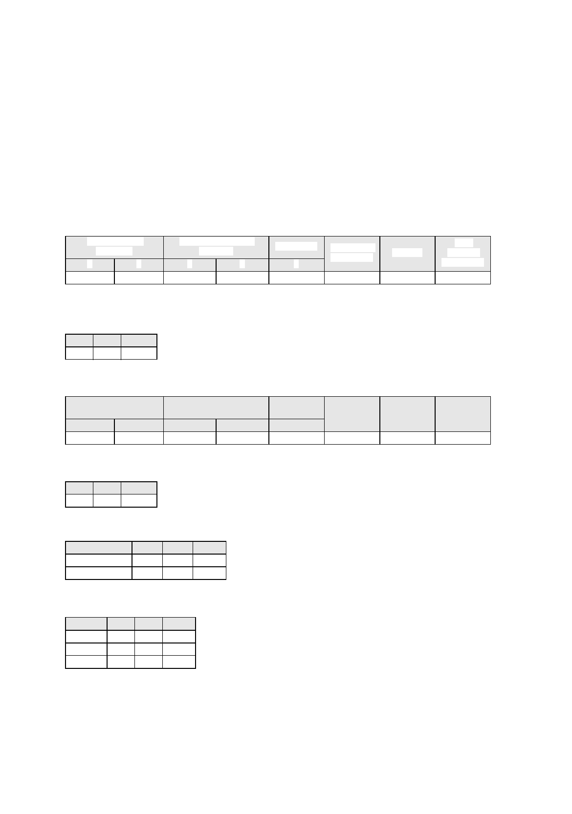
Have you entered all values correctly? Compare the solutions below (see also Fig. 17.3.7 on
page 17-41):
Di
mens
i
ons o
f
th
e
PCB
(
page
17
-
43
)
Vector (0.0) -->
Corner_1:
Vector Corner_1 -->
Corner_2
PCB height
PP position
recognition
Ink spot
PCB
position
recognition
X Y X Y h
-5 -5 335 272 1.5 no no no
Offset values of the first cluster (page 17-45)
X Y
Angle
10 10 0
Dimensions of the first cluster (page 17-45)
Vector (0,0) -->
Corner_1:
Vector Corner_1 -->
Corner_2
PCB height
PP position
recognition
Ink spot
PCB
position
recognition
X Y X Y h
0 0 150 116 no no yes
Offset values of the first single circuit (page 17-47)
X Y
Angle
15 15 0
Offset values of the duplicated single circuits (page 17-49)
Single circuit X Y ] Angle
board_2 60 15 0
baord_3 105 15 0
Offset values of the duplicated clusters (page 17-49)
Cluster X Y Angle
pattern_2 165 10 0
pattern_3 160 252 180
pattern_4 315 252 180