00195941-03-UM SiplaceCA-EN.pdf - 第150页
3 Technical Data User Manual SIPLACE CA 3.7 SIPLACE Wafer System (SWS) Edition 08/2011 EN 150 In order to support the whole rang e of process-or iented functions, the fo llowi ng options are avail- able: – W afer map sys…

User Manual SIPLACE CA 3 Technical Data
Edition 08/2011 EN 3.7 SIPLACE Wafer System (SWS)
149
3.7.1 SIPLACE Wafer System (SWS) Function
The new SWS provides a fully automatic wafer and chip handling system. This is fully integrated
into one of the SIPLACE CA placement system locations. Every location can be equipped (with
restrictions) with a SWS or a X-table.
The SWS functions like a feeder for the SIPLACE system and transports the dies from the wafer
to a single, fixed pickup position for the placement head. The placement head picks up the die at
the SWS and places it on the PCB in the same way as during SMD handling.
The SWS appears in SIPLACE Pro as an X feeder with a special feeder type. The SIPLACE sys-
tem is programmed as usual for the SIPLACE X series. Die handling is programmed at a separate
terminal on the SWS. The main parameters to be programmed are as follows:
– Wafer and die dimensions
– Magazine type
– Wafer frame type
– Die recognition
– Die ejection parameters
– Wafer map system
– Link to the component programmed in SIPLACE Pro
3.7.2 Basic SWS Functions
The basic components for die handling are the wafer table, the ejection system, the flip unit and
the control unit including the relevant software.
The wafer with the relevant die is loaded from the magazine and fixed on the wafer table. The wa-
fer table places the die above the ejection system where the die is separated from the foil and
handed over to the flip unit. The flip unit rotates the die by 180° and provides it for pickup by the
placement head.
The SIPLACE CA uses a high-precision SIPLACE placement head, which has been specially de-
signed for high accuracy, to achieve the set 35 µm at 3 Sigma for normal and 25 µm at 3 Sigma
for restricted conditions (for restrictions see "Scope of Delivery").
NOTE 3
All moveable positioning axes in the SWS are servo axes!
3 Technical Data User Manual SIPLACE CA
3.7 SIPLACE Wafer System (SWS) Edition 08/2011 EN
150
In order to support the whole range of process-oriented functions, the following options are avail-
able:
– Wafer map system
– Linear dipping unit
– Die attach unit:
– Small die kit (on request)
– Barcode scanner
– Wafer stretcher
– Inspection camera
3.7.3 Basic Die Presentation Process
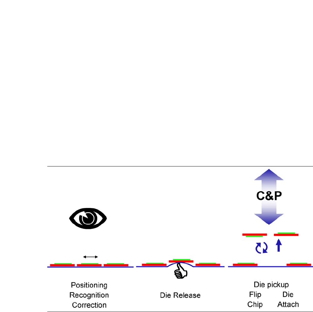
The basic die presentation process supported by the SWS can be divided into 3 main steps:
– Die recognition and positioning for ejection (inc. inkspot recognition or wafer map)
– Ejection process
– Pickup for die attach or flip chip processing.
Fig. 3.7 - 2 Basic die presentation process
There are two main placement variants - flip chip and die attach.
User Manual SIPLACE CA 3 Technical Data
Edition 08/2011 EN 3.7 SIPLACE Wafer System (SWS)
151
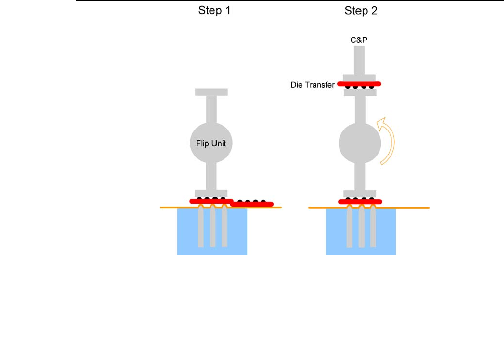
3.7.3.1 Flip Chip Process
The flip chip process is the standard method for SWS. This involves rotating the die by 180° before
it is placed on the board (face down placement).
The flip chip process is a method which is rapidly gaining in popularity. This process is primarily
used for consumer electronics assemblies (e.g. processors, graphics processors, memory).
The inputs/outputs (I/A) of the dies are directly connected to the PCB which results in several ben-
efits compared to the classical die attach process:
Less space required
Faster signal transfer
Higher I/O density per component
Fig. 3.7 - 3 Flip Chip Process
The flip chip process steps are:
– Step 1: Die release
– Step 2: The die is rotated by 180° and is passed on to the placement head. At the same time
the next die is picked up by the second nozzle of the flip unit.