00195941-03-UM SiplaceCA-EN.pdf - 第152页
3 Technical Data User Manual SIPLACE CA 3.7 SIPLACE Wafer System (SWS) Edition 08/2011 EN 152 3.7.3.2 Die Att ach Process The optional die attach unit is used for the die atta ch process. In this method, the die is place…
User Manual SIPLACE CA 3 Technical Data
Edition 08/2011 EN 3.7 SIPLACE Wafer System (SWS)
151
3.7.3.1 Flip Chip Process
The flip chip process is the standard method for SWS. This involves rotating the die by 180° before
it is placed on the board (face down placement).
The flip chip process is a method which is rapidly gaining in popularity. This process is primarily
used for consumer electronics assemblies (e.g. processors, graphics processors, memory).
The inputs/outputs (I/A) of the dies are directly connected to the PCB which results in several ben-
efits compared to the classical die attach process:
Less space required
Faster signal transfer
Higher I/O density per component
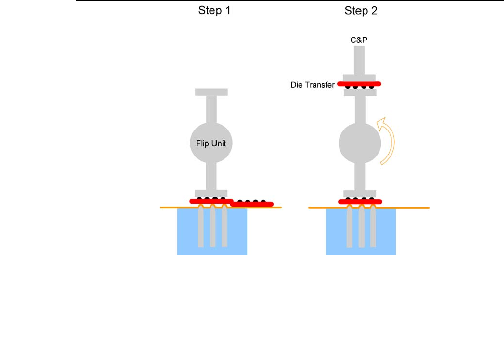
Fig. 3.7 - 3 Flip Chip Process
The flip chip process steps are:
– Step 1: Die release
– Step 2: The die is rotated by 180° and is passed on to the placement head. At the same time
the next die is picked up by the second nozzle of the flip unit.
3 Technical Data User Manual SIPLACE CA
3.7 SIPLACE Wafer System (SWS) Edition 08/2011 EN
152
3.7.3.2 Die Attach Process
The optional die attach unit is used for the die attach process.
In this method, the die is placed in the same bottom/top orientation as it was on the wafer foil
("face-up" placement).
Die attach is the conventional die placement procedure. It requires an additional step in order to
establish the connection from the die to the board (wire connections).
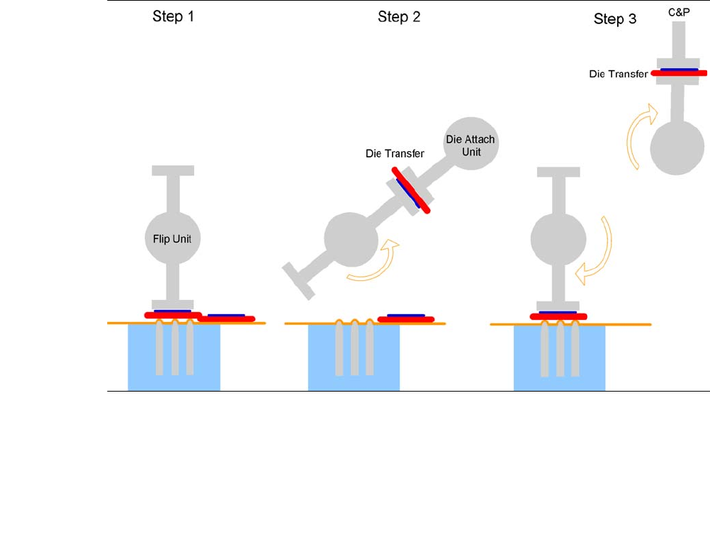
Fig. 3.7 - 4 Die attach process steps
The die attach process steps are:
– Step 1: Die release
– Step 2: The die is rotated by approx. 130°and handed over to the die attach unit.
– Step 3: The die attach unit rotates the die into pickup position and passes it on the placement
head. At the same time the flip unit picks up the next die.
User Manual SIPLACE CA 3 Technical Data
Edition 08/2011 EN 3.7 SIPLACE Wafer System (SWS)
153
3.7.3.3 Die Recognition and Positioning
The wafers are fixed to the wafer foil with a specific position and angular tolerance.
For this reason it is not possible to place the die in the center of the ejection unit without a recog-
nition and correction process. This is particularly important for small dies, in order to ensure reli-
able ejection.
Furthermore, you may need to process only a selection of dies. Such a selection can be done by
an inkdot marking on "bad" dies or with a wafer map file of the respective wafer.
The following equipment is required for this step:
2 axis wafer table for positioning
Wafer- camera system for die recognition and optional inkspot recognition
Optional wafer map system
3.7.3.4 Ejection Process
If the die is centered above the ejection system it can be separated from the wafer foil by means
of needles and passed on to the flip unit. While the needles release the die from the foil, the wafer
foil is moved towards the ejection system by means of suction.
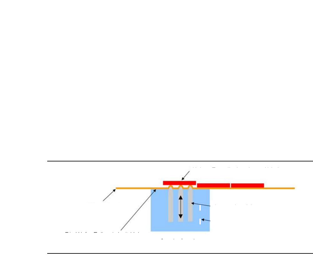
Fig. 3.7 - 5 Die provisioning process
The following equipment is required for this method:
– Ejection system with replaceable ejector tool
Active component - ready for pickup
Ejection needle
Vacuum cap
Ejection System
Waferf foil
The wafer foil is sucked up to the
vacuum cap by a vacuum