00195941-03-UM SiplaceCA-EN.pdf - 第236页
3 Technical Data User Manual SIPLACE CA 3.14 PCB Single Conveyor Edition 0 8/2011 EN 236 3.14.4.1 PCB-W arpag e During T ransport PCB warp age across the d irection of tra vel max. 1 % of the PCB diagonal, but not exce e…

User Manual SIPLACE CA 3 Technical Data
Edition 08/2011 EN 3.14 PCB Single Conveyor
235
3.14.3 Functional Description
For placement, the PCB is clamped from below. The distance between the top of the PCB and the
placement head thus remains unchanged for each PCB, and is not dependent on the thickness of
the PCB. The placement rate is thus independent of the PCB thickness. The PCB fiducial center-
ing can also be optimized. By the constant space between PCB-surface and PCB-camera the fo-
cus of the PCB-camera is constantly adjusted sharp on the PCB-surface. The PCB fiducial
contours are optimally mapped on the CCD chip of the PCB camera.
The width of the circuit board conveyor is set and monitored by an integral control circuit. It can
be selected by calling up the program. The control circuit then actuates the stepping motors until
the desired width is reached. The width adjustment is therefore independent of other machine
components.
The conveyor height can be selected on the placement machine, so that this can be integrated
into lines supporting conveyor heights of 830, 900, 930 or 950 mm.
The communication between the PCB conveyors and the individual placement machines is via a
SMEMA interface or an optional Siemens interface.
The fixed transport side can be located on the left or right for both the dual conveyor and the single
conveyor. With this conveyor, the fixed side can be easily switched from right to left and vice versa
using the station software.
The circuit board conveyor is monitored and controlled with optical sensors. If the PCB reaches
the placement area and passes the light barrier, it is slowed down. A laser light barrier determines
the position of the board. As soon as the circuit board has reached its target position, the conveyor
belt is stopped and the board is clamped from below.
3.14.4 PCB Warpage
NOTE 3
In order to adhere to the set board curvature, use the vacuum tool for thin substrates (less than
0.7 mm) .
NOTE 3
The vacuum tool is not always essential. However, it is needed for use with thin substrates, to
ensure placement accuracy and error-free handling.
3 Technical Data User Manual SIPLACE CA
3.14 PCB Single Conveyor Edition 08/2011 EN
236
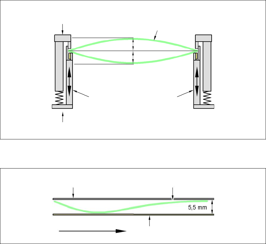
3.14.4.1 PCB-Warpage During Transport
PCB warpage across the direction of travel max. 1 % of the PCB diagonal, but not exceeding 0.5
mm
3
PCB warpage in direction of travel + PCB thickness < 5.5 mm
3
3
Fixed clamped edge
Movable clamping device
Printed circuit board
Conveyor side
0.5 mm
0.5 mm
Fixed clamped edge
Conveyor belt
Printed circuit board
PCB transport direc-
tion
User Manual SIPLACE CA 3 Technical Data
Edition 08/2011 EN 3.14 PCB Single Conveyor
237
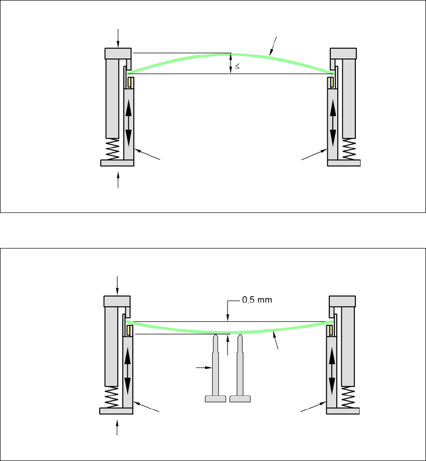
3.14.4.2 PCB-Warpage during Placement
In case of a warpage of 0,5 mm problems can occur during focusing of local fiducials and inkdots
in the PCB-center. The digital camera's focus is 2 mm. When all the tolerances are taken into ac-
count, this value is reduced to 1.5 mm. Also note that the component height is reduced by the war-
page.
3
3
PCB warpage down, max. 0.5 mm
3
Use magnetic pin supports to achieve this value.
Movable clamping device
Fixed clamped edge
Printed circuit board
conveyor side
0.5 mm
Printed circuit board
Magnetic pin
support
Movable clamping device
Fixed clamped edge
Conveyor side