ASM锡膏检查机_ProcessLens_EN性能参数 - 第11页
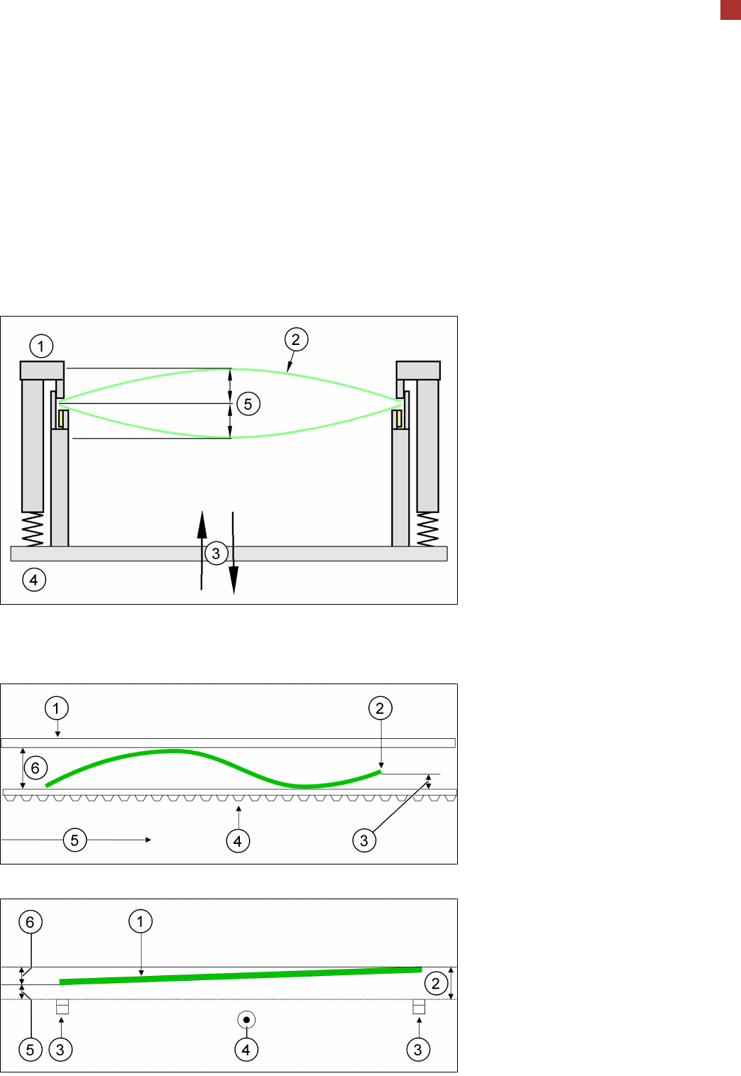
ASM ProcessLens PCB warpage 11 PCB warpage PCB warpage on the conveyor PCB warpage across the direction of travel max. 1% of the PCB diagonal, but not exceeding ±5mm. 1. Fixed clamped edge 2. Printed circuit board 3. M…
ASM ProcessLens
Technical data
10
Technical data
Solder paste inspection capabilities
Measurement Shadow-free
Paste measurement functions Volume, area, height, X-and Y-offset, shape,
bridging, coplanarity
Maximum paste height 1000 μm
Minimum paste size 90 μm x 130 μm
Minimum paste pitch 75 μm
Height repeatability on solder paste ≤ 1 μm at ± 3 σ
Volume repeatability on solder paste ≤ 3 % at ± 3 σ
Area repeatability on solder paste ≤ 3 % at ± 3 σ
Gage Repeatability and Reproducibility (GRR) ≤ 10 %
Program generation specifications
Program generation < 10 min.
Offline programming available
Supported Gerber formats RS-274X
The Hermes Standard
IPC-Hermes-9852
A protocol for advanced development of Industry 4.0 in electronics produc-
tion
The Hermes Standard, also published as IPC-HERMES-9852, is a non-proprietary
open protocol, based on TCP / IP and XML. This boosts the exchange of PCB-rel-
evant data between the various machines in the electronics production lines. The
Hermes Standard was initiated, developed and established and is still managed by
a group of leading equipment manufacturers, who share their know-how to
achieve a significant step towards advanced process integration. It has been re-
cognized by IPC as the next generation solution for IPC-SMEMA-9851, normally
known as "SMEMA standard".
The founding and defining body The Hermes Standard Initiative is available to all
equipment providers wanting to actively participate in using the benefits of Industry
4.0 for their customers.
ASM ProcessLens
PCB warpage
11
PCB warpage
PCB warpage on the conveyor
PCB warpage across the direction of travel max. 1% of the PCB diagonal, but not exceeding ±5mm.
1. Fixed clamped edge
2. Printed circuit board
3. Movable clamping device
4. Conveyor rail
5. +/- 4.5 mm
PCB warpage in the direction of transport + PCB thickness < 5.5 mm. Bending up of board edge max. 2.5 mm.
1. Fixed clamped edge
2. Front board edge
3. Max. 2.5 mm
4. Conveyor belt
5. PCB transport direction
6. 5.5 mm
1. Front board edge
2. Max. 2.5 mm
3. Conveyor rail
4. PCB transport direction
5. Max. 2.5 mm
6. Max. 3 mm

ASM ProcessLens
PCB warpage
12
PCB warpage
Maximum PCB warpage allowed during processing of the board
There is active PCB warpage measurement and tracking during the inspection so that images remain in sharp
focus, ensuring best height measurement accuracy on the market.
1. Fixed clamped edge
2. Printed circuit board
3. ≤ 2 mm
4. Movable clamping device
5. Conveyor rail
PCB warpage down, max. 4.5 mm
1. Fixed clamped edge
2. 0.5 mm
3. Printed circuit board
4. Magnetic pin support
5. Movable clamping device
6. Conveyor rail
► Use magnetic pin supports to achieve this value.