ASM锡膏检查机_ProcessLens_EN性能参数 - 第12页
ASM ProcessLens PCB warpage 12 PCB warpage Maximum PCB warpage allowed during processing of the board There is active PCB warpage measurement and tracking during the inspection so that images remain in sharp focus, ensur…
ASM ProcessLens
PCB warpage
11
PCB warpage
PCB warpage on the conveyor
PCB warpage across the direction of travel max. 1% of the PCB diagonal, but not exceeding ±5mm.
1. Fixed clamped edge
2. Printed circuit board
3. Movable clamping device
4. Conveyor rail
5. +/- 4.5 mm
PCB warpage in the direction of transport + PCB thickness < 5.5 mm. Bending up of board edge max. 2.5 mm.
1. Fixed clamped edge
2. Front board edge
3. Max. 2.5 mm
4. Conveyor belt
5. PCB transport direction
6. 5.5 mm
1. Front board edge
2. Max. 2.5 mm
3. Conveyor rail
4. PCB transport direction
5. Max. 2.5 mm
6. Max. 3 mm

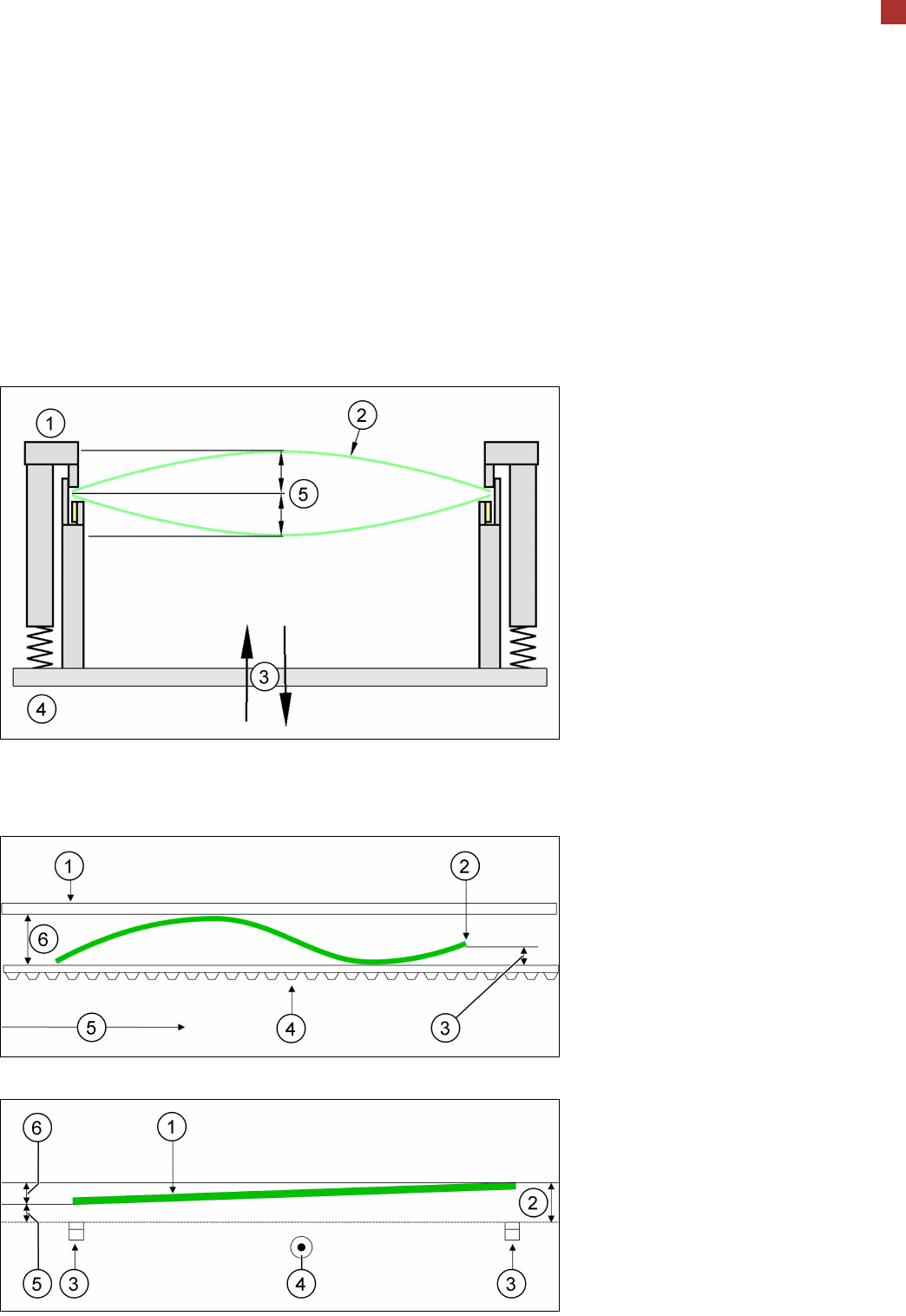
ASM ProcessLens
PCB warpage
12
PCB warpage
Maximum PCB warpage allowed during processing of the board
There is active PCB warpage measurement and tracking during the inspection so that images remain in sharp
focus, ensuring best height measurement accuracy on the market.
1. Fixed clamped edge
2. Printed circuit board
3. ≤ 2 mm
4. Movable clamping device
5. Conveyor rail
PCB warpage down, max. 4.5 mm
1. Fixed clamped edge
2. 0.5 mm
3. Printed circuit board
4. Magnetic pin support
5. Movable clamping device
6. Conveyor rail
► Use magnetic pin supports to achieve this value.
ASM ProcessLens
Overview of languages
13
Overview of languages
Documentation package Station software from 4.1.0.8 onwards
German X X
English X X
Italian X On request
Czech X X
Polish X On request
Chinese X X
Japanese X X
Other languages can be realized on request.