IPC-A-610C(电子组装件的验收条件).pdf - 第361页
IPC-2221 – 6.3.2 B2-External Conductors, Uncoated, Sea Level to 3050 m Electrical clearance requirements for uncoated external conductors are significantly greater than for conductors that will be protected from external…
NOTE: Appendix A is quoted from IPC-2221 Generic Stan-
dard on Printed Board Design (February 1998) and is pro-
vided for information only. It is current as of publication
date of this document. The user has the responsibility to
determine the most current revision level of IPC-2221 and
specify the specific application to their product. Paragraph
and table numbers are from IPC-2221.
The following statement from IPC-2221 applies to this Appen-
dix ONLY: 1.4 Interpretation – ‘‘Shall,’’ the imperative form
of the verb, is used throughout this standard [IPC-A-610C
Appendix A] whenever a requirement is intended to express a
provision that is mandatory.
IPC-2221 –
6.3 Electrical Clearance Spacing between
conductors on individual layers should be maximized when-
ever possible. The minimum spacing between conductors,
between conductive patterns, layer to layer conductive
spaces (z-axis), and between conductive materials (such as
conductive markings or mounting hardware) and conductors
shall be in accordance with Table 6-1, and defined on the
master drawing. For additional information on process allow-
ances effecting electrical clearance, see Section 10.
When mixed voltages appear on the same board and they
require separate electrical testing, the specific areas shall be
identified on the master drawing or appropriate test specifica-
tion. When employing high voltages and especially AC and
pulsed voltages greater than 200 volts potential, the dielectric
constant and capacitive division effect of the material must be
considered in conjunction with the recommended spacing.
For voltages greater than 500V, the (per volt) table values
must be added to the 500V values. For example, the electri-
cal spacing for a Type B1 board with 600V is calculated as:
600V - 500V = 100V
0.25 mm + (100V x 0.0025 mm)
= 0.50 mm clearance
When, due to the criticality of the design, the use of other
conductor spacings is being considered, the conductor spac-
ing on individual layers (same plane) shall be made larger
than the minimum spacing required by Table 6-1 whenever
possible. Board layout should be planned to allow for the
maximum spacing between external layer conductive areas
associated with high impedance or high voltage circuits. This
will minimize electrical leakage problems resulting from con-
densed moisture or high humidity. Complete reliance on coat-
ings to maintain high surface resistance between conductors
shall be avoided.
IPC-2221 –
6.3.1 B1-Internal Conductors Internal
conductor-to-conductor, and conductor-to-plated-through
hole electrical clearance requirements at any elevation. See
Table 6-1.
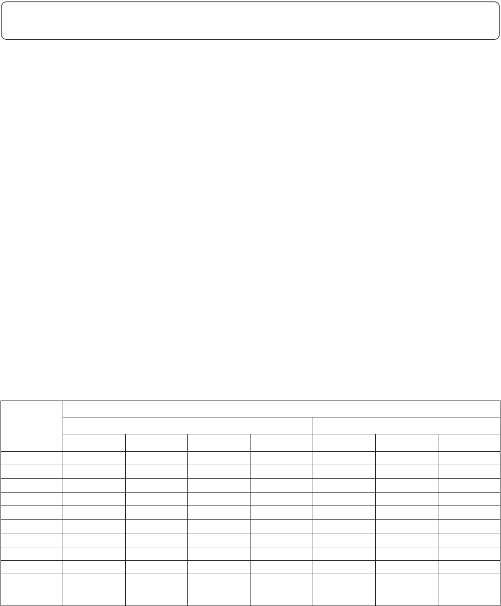
IPC-2221 –
Table 6-1 Electrical Conductor Spacing
Voltage
Between
Conductors
(DC or AC
Peaks)
Minimum Spacing
Bare Board Assembly
B1 B2 B3 B4 A5 A6 A7
0-15 0.05 mm 0.1 mm 0.1 mm 0.05 mm 0.13 mm 0.13 mm 0.13 mm
16-30 0.05 mm 0.1 mm 0.1 mm 0.05 mm 0.13 mm 0.25 mm 0.13 mm
31-50 0.1 mm 0.6 mm 0.6 mm 0.13 mm 0.13 mm 0.4 mm 0.13 mm
51-100 0.1 mm 0.6 mm 1.5 mm 0.13 mm 0.13 mm 0.5 mm 0.13 mm
101-150 0.2 mm 0.6 mm 3.2 mm 0.4 mm 0.4 mm 0.8 mm 0.4 mm
151-170 0.2 mm 1.25 mm 3.2 mm 0.4 mm 0.4 mm 0.8 mm 0.4 mm
171-250 0.2 mm 1.25 mm 6.4 mm 0.4 mm 0.4 mm 0.8 mm 0.4 mm
251-300 0.2 mm 1.25 mm 12.5 mm 0.4 mm 0.4 mm 0.8 mm 0.8 mm
301-500 0.25 mm 2.5 mm 12.5 mm 0.8 mm 0.8 mm 1.5 mm 0.8 mm
> 500
See para. 6.3
for calc.
0.0025 mm
/volt
0.005 mm
/volt
0.025 mm
/volt
0.00305 mm
/volt
0.00305 mm
/volt
0.00305 mm
/volt
0.00305 mm
/volt
B1 - Internal Conductors
B2 - External Conductors, uncoated, sea level to 3050 m
B3 - External Conductors, uncoated, over 3050 m
B4 - External Conductors, with permanent polymer coating (any elevation)
A5 - External Conductors, with conformal coating over assembly (any elevation)
A6 - External Component lead/termination, uncoated
A7 - External Component lead termination, with conformal coating (any elevation)
Appendix A
Electrical Conductor Spacing
A-1IPC-A-610C January 2000

IPC-2221 –
6.3.2 B2-External Conductors, Uncoated,
Sea Level to 3050 m
Electrical clearance requirements for
uncoated external conductors are significantly greater than for
conductors that will be protected from external contaminants
with conformal coating. If the assembled end product is not
intended to be conformally coated, the bare board conductor
spacing shall require the spacing specified in this category for
applications from sea level to an elevation of 3050 m. See
Table 6-1.
IPC-2221 –
6.3.3 B3-External Conductors, Uncoated,
Over 3050 m
External conductors on uncoated bare board
applications over 3050 m require even greater electrical spac-
ings than those identified in category B2. See Table 6-1.
IPC-2221 –
6.3.4 B4-External Conductors, with Perma-
nent Polymer Coating (Any Elevation)
When the final
assembled board will not be conformally coated, a permanent
polymer coating over the conductors on the bare board will
allow for conductor spacings less than that of the uncoated
boards defined by category B2 and B3. The assembly electri-
cal clearances of lands and leads that are not conformally
coated require the electrical clearance requirements stated in
category A6 (see Table 6-1). This configuration is not appli-
cable for any application requiring protection from harsh,
humid, contaminated environments.
Typical applications are computers, office equipment, and
communication equipment, bare boards operating in con-
trolled environments in which the bare boards have a perma-
nent polymer coating on both sides. After they are assembled
and soldered the boards are not conformal coated, leaving
the solder joint and soldered land uncoated.
Note: All conductors, except for soldering lands, must be
completely coated in order to ensure the electrical clearance
requirements in this category for coated conductors.
IPC-2221 –
6.3.5 A5-External Conductors, with Confor-
mal Coating Over Assembly (Any Elevation)
Externalcon-
ductors that are intended to be conformal coated in the final
assembled configuration, for applications at any elevation, will
require the electrical clearances specified in this category.
Typical applications are military products where the entire final
assembly will be conformal coated. Permanent polymer coat-
ings are not normally used, except for possible use as a sol-
der resist. However, the compatibility of polymer coating and
conformal coating must be considered, if used in combina-
tion.
IPC-2221 –
6.3.6 A6-External Component Lead/
Termination, Uncoated
External component leads and ter-
minations, that are not conformal coated, require electrical
clearances stated in this category.
Typical applications are as previously stated in category B4.
The B4/A6 combination is most commonly used in commer-
cial, non-harsh environment applications in order to obtain the
benefit of high conductor density protected with permanent
polymer coating (also solder resist), or where the accessibility
to components for rework and repair is not required.
IPC-2221 –
6.3.7 A7-External Component Lead/
Termination, with Conformal Coating (Any Elevation)
As
in exposed conductors versus coated conductors on bare
board, the electrical clearances used on coated component
leads and terminations are less than for uncoated leads and
terminations.
Appendix A
Electrical Conductor Spacing (cont.)
A-2 IPC-A-610CJanuary 2000
Standard Improvement Form IPC-A-610C
The purpose of this form is to provide the
Technical Committee of IPC with input
from the industry regarding usage of
the subject standard.
Individuals or companies are invited to
submit comments to IPC. All comments
will be collected and dispersed to the
appropriate committee(s).
If you can provide input, please complete
this form and return to:
IPC
2215 Sanders Road
Northbrook, IL 60062-6135
Fax 847 509.9798
1. I recommend changes to the following:
Requirement, paragraph number
Test Method number , paragraph number
The referenced paragraph number has proven to be:
Unclear Too Rigid In Error
Other
2. Recommendations for correction:
3. Other suggestions for document improvement:
Submitted by:
Name Telephone
Company E-mail
Address
City/State/Zip Date
ASSOCIATION CONNECTING
ELECTRONICS INDUSTRIES
®