IPC-TM-650 EN 2022 试验方法--.pdf - 第106页
IPC-TM-650 Number Subject Date Revision Page 2 of 2 4/73 2.3.1 Chemical Processing, Suitable Processing Material 5.3.4 Drill 1.5 mm holes in the pads of the 3 mm lines with good fabricating practice. 5.3.5 Remove the dev…
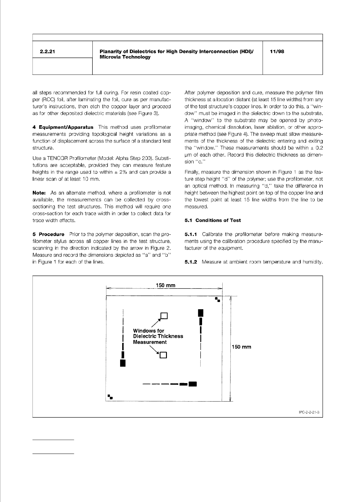
Figure 3 Pattern of One Test Board Showing Three Test Substructures (Board is 150 mm sq.)
IPC-TM-650
Number
Subject Date
Revision
Page 2 of 4
2.2.21
Planarity
of
Dielectrics
for
High
Density
Interconnection
(HDI)/
Microvia
Technology
11/98
all
steps
recommended
for
full
curing.
For
resin
coated
cop¬
per
(RCC)
foil,
after
laminating
the
foil,
cure
as
per
manufac¬
turer's
instructions,
then
etch
the
copper
layer
and
proceed
as
for
other
deposited
dielectric
materials
(see
Figure
3).
4
Equipment/Apparatus
This
method
uses
profilometer
measurements
providing
topological
height
variations
as
a
function
of
displacement
across
the
surface
of
a
standard
test
structure.
Use
a
TENCOR
Profilometer
(Model:
Alpha
Step
200).
Substi¬
tutions
are
acceptable,
provided
they
can
measure
feature
heights
in
the
range
used
to
within
土
2%
and
can
provide
a
linear
scan
of
at
least
10
mm.
Note:
As
an
alternate
method,
where
a
profilometer
is
not
available,
the
measurements
can
be
collected
by
cross¬
sectioning
the
test
structures.
This
method
will
require
one
cross-section
for
each
trace
width
in
order
to
collect
data
for
trace
width
effects.
5
Procedure
Prior
to
the
polymer
deposition,
scan
the
pro¬
filometer
stylus
across
all
copper
lines
in
the
test
structure,
scanning
in
the
direction
indicated
by
the
arrow
in
Figure
2.
Measure
and
record
the
dimensions
depicted
as
“a”
and
"b”
in
Figure
1
for
each
of
the
lines.
After
polymer
deposition
and
cure,
measure
the
polymer
film
thickness
at
a
location
distant
(at
least
1
5
line
widths)
from
any
of
the
test
structure's
copper
lines.
In
order
to
do
this,
a
''win-
dow!,
must
be
imaged
in
the
dielectric
down
to
the
substrate.
A
,(window"
to
the
substrate
may
be
opened
by
photo¬
imaging,
chemical
dissolution,
laser
ablation,
or
other
appro¬
priate
method
(see
Figure
4).
The
sweep
must
allow
measure¬
ments
of
the
thickness
of
the
dielectric
entering
and
exiting
the
''window.”
These
measurements
should
be
within
±
0.2
pm
of
each
other.
Record
this
dielectric
thickness
as
dimen-
sion
"c."
Finally,
measure
the
dimension
shown
in
Figure
1
as
the
fea¬
ture
step
height
"cT
of
the
polymer;
use
the
profilometer,
not
an
optical
method.
In
measuring
"dj
take
the
difference
in
height
between
the
highest
point
on
top
of
the
copper
line
and
the
lowest
point
at
least
15
line
widths
from
the
line
to
be
measured.
5.1
Conditions
of
Test
5.1.1
Calibrate
the
profilometer
before
making
measure¬
ments
using
the
calibration
procedure
specified
by
the
manu¬
facturer
of
the
equipment.
5.1.2
Measure
at
ambient
room
temperature
and
humidity.
I
PC-2-2-21
-3
IPC-TM-650
Number
Subject Date
Revision
Page 2 of 2
4/73
2.3.1
Chemical
Processing,
Suitable
Processing
Material
5.3.4
Drill
1.5
mm
holes
in
the
pads
of
the
3
mm
lines
with
good
fabricating
practice.
5.3.5
Remove
the
developed
KPR
by
rubbing
the
pattern
lightly
with
cold
trichlorethylene
liquid.
Rinse
in
water.
Scrub
the
specimens
with
FFF
pumice
and
water
with
a
strong
bristle
brush.
5.3.6
Plate
(this
is
simulated
plating)
per
MIL-P-1
3949.
5.3.7
Deoxidize
by
dipping
in
10%
hydrochloric
acid
for
two
minutes
and
wash
in
running
water
for
five
minutes.
Dry
30
minutes,
minimum,
at
105℃
to1
10℃.
5.3.8
Coat
the
etched
copper
surface
with
white
petrola¬
tum.
Specimens
shall
be
immersed
horizontally
in
solder
6.5
mm
below
the
surface
for
20
土
1
seconds
at
260℃
+5/-0℃
measured
25
mm
below
the
surface.
5.3.9
Remove
the
petrolatum
from
the
surface
of
the
speci¬
men
with
a
two
minute
scrub
in
cold
trichlorethylene,
followed
by
a
one
minute
rinse
in
hot
trichlorethylene.
5.3.10
Inspect
the
surface
for
weave
exposure,
measling,
crazing,
resin
loss,
delamination,
and
blistering.
5.3.11
Test
four
1
mm
lines
on
the
specimen
for
peel
strength
per
MIL-P-13949,
reporting
the
average
value
for
the
four
lines.
Chemical Concentration Temperature
Chemical Concentration Temperature
The Institute for Interconnecting and Packaging Electronic Circuits
2215 Sanders Road • Northbrook, IL 60062-6135
Material in this Test Methods Manual was voluntarily established by Technical Committees of the IPC. This material is advisory only
and its use or adaptation is entirely voluntary. IPC disclaims all liability of any kind as to the use, application, or adaptation of this
material. Users are also wholly responsible for protecting themselves against all claims or liabilities for patent infringement.
Equipment referenced is for the convenience of the user and does not imply endorsement by the IPC.
Page 1 of 1
IPC-TM-650
TEST
METHODS
MANUAL
1
.0
Scope
This
method
evaluates
the
chemical
cleanability
of
metal-clad
laminate
surfaces
of
oxidation
and
anti-oxidation
protective
coatings.
2
.0
Applicable
Document
None.
3
.0
Test
Specimen
The
size
of
the
test
specimen
shall
be
determined
by
the
post
etching
tests
to
be
performed.
4
.0
Apparatus
4.1
Standard
conveyorized
spray
cleaning
modules
or
suit¬
able
laboratory
equipment.
4.2
Personal
safety
equipment
needed
to
perform
this
test
are
as
follows:
rubber
or
polyethylene
gloves,
plastic
or
coated
apron
and
safety
goggles.
4.3
Chemicals
4.3.1
Method
A
~
Sodium
Persulfate
Cleaner/
Degreaser
Sodium
Persulfate
Per
manufacturer's
recommended
limits
1.5
Ibs/gal
(土
0.5
Ib/gal)
As
recommended
100°±5°F
(38°
±
3
℃)
4.3.2
Method
B
一
Ammonium
Persulfate
Cleaner/
Degreaser
Ammonium
Persulfate
Tech
Grade
Per
manufacturer's
recommended
limits
2.0
Ibs/gal
(±
0.5
Ib/gal)
As
recommended
100°F
Max
Number
2.3.1.
1
Subject
Chemical
Cleaning
of
Metal-Clad
Laminate
Date
Revision
5/86
B
Originating
Task
Group
N/A
5.0
Procedure
5.1
Specimen
Preparation
Shear
the
material
to
the
required
specimen
size
and
remove
the
rough
edges
from
the
specimen
by
sanding
or
other
suitable
means.
5.2
Cleaning
5.2.1
Conveyorized
Spray
Cleaning
Process
the
speci¬
men
through
the
conveyorized
modules
at
a
speed
which
will
permit
30
±
5
seconds
of
exposure
to
the
micro
etching
solu¬
tion.
Rinse
specimens
with
deionized
water
for
1-2
minutes
after
micro
etching.
5.2.2
Laboratory
Cleaning
Place
the
specimen
in
a
cleaner/degreaser
solution
and
gently
agitate
for
30
±
5
sec¬
onds.
Remove
the
specimen
and
flush
with
tap
water.
Next
place
the
specimen
in
a
micro
etch
solution
for
30
±
5
sec¬
onds
and
vigorously
agitate.
Remove
the
specimen
and
flush
with
deionized
water
for
1
-2
minutes.
5.3
Surface
Evaluation
The
metal
cladding
on
the
test
specimen
shall
be
cleaned
to
a
uniform
matte
finish.
Deionized
or
distilled
water
poured
on
the
metal
surface
does
not
bead
or
form
puddles.
6.0
Notes
6.1
Sodium
persulfate
solution
shall
be
replaced
if
the
cop¬
per
concentration
exceeds
3.0
oz/gal
(22.5
gal).
6.2
Solution
spray
from
nozzles
should
be
checked
for
uni¬
formity
across
the
specimen.