IPC-TM-650 EN 2022 试验方法--.pdf - 第272页
Figure 2 Aid to Evaluation IPC-TM-650 Number Subject Date Revision Page 3 of 3 Solderability, Edge Dip Method 2.4.12 6/91
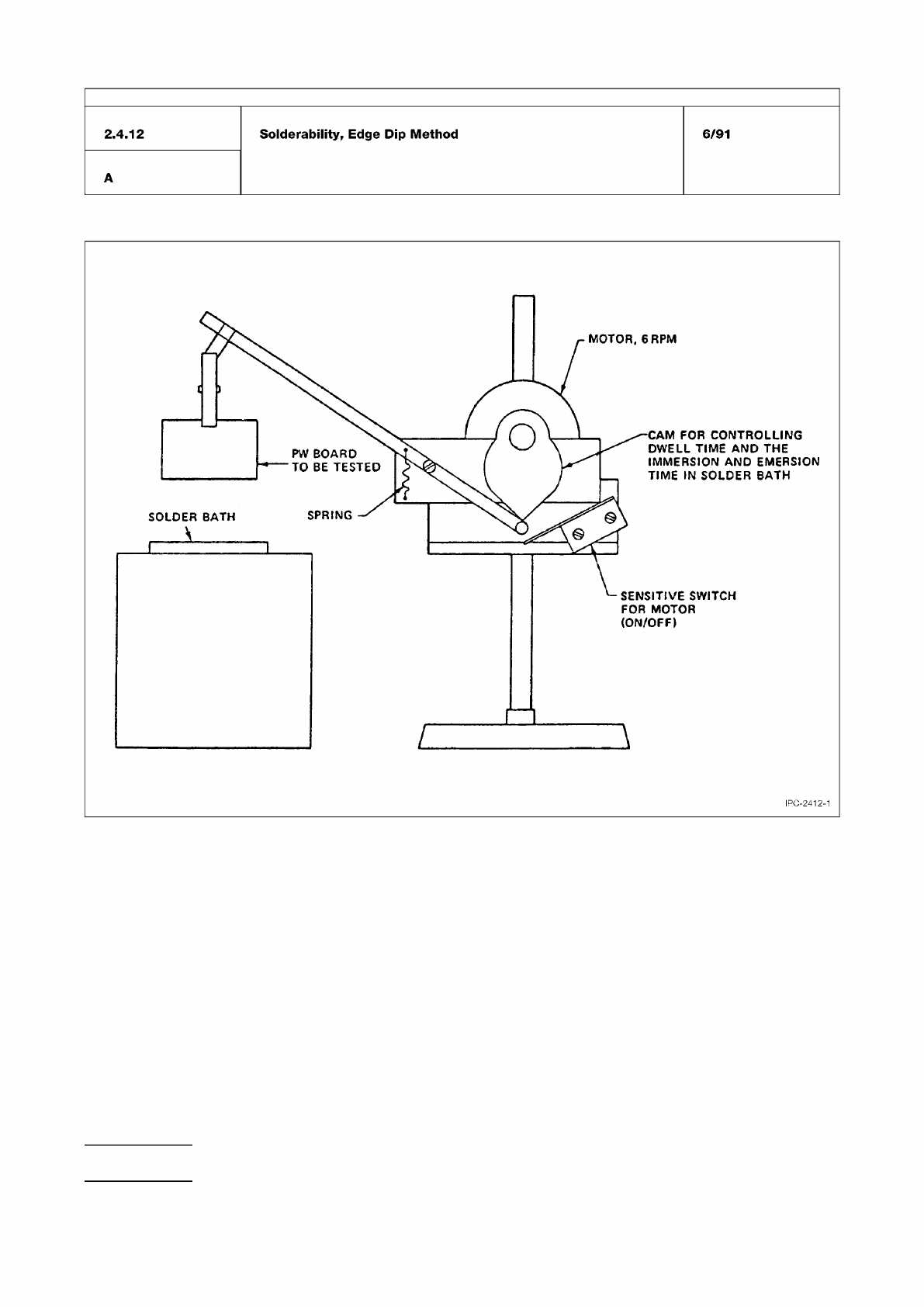
Figure 1 Suggested Dipping Device
IPC-TM-650
Number
Subject Date
Revision
Page 2 of 3
Solderability,
Edge
Dip
Method
2.4.12
A
6/91
IPC-2412-1
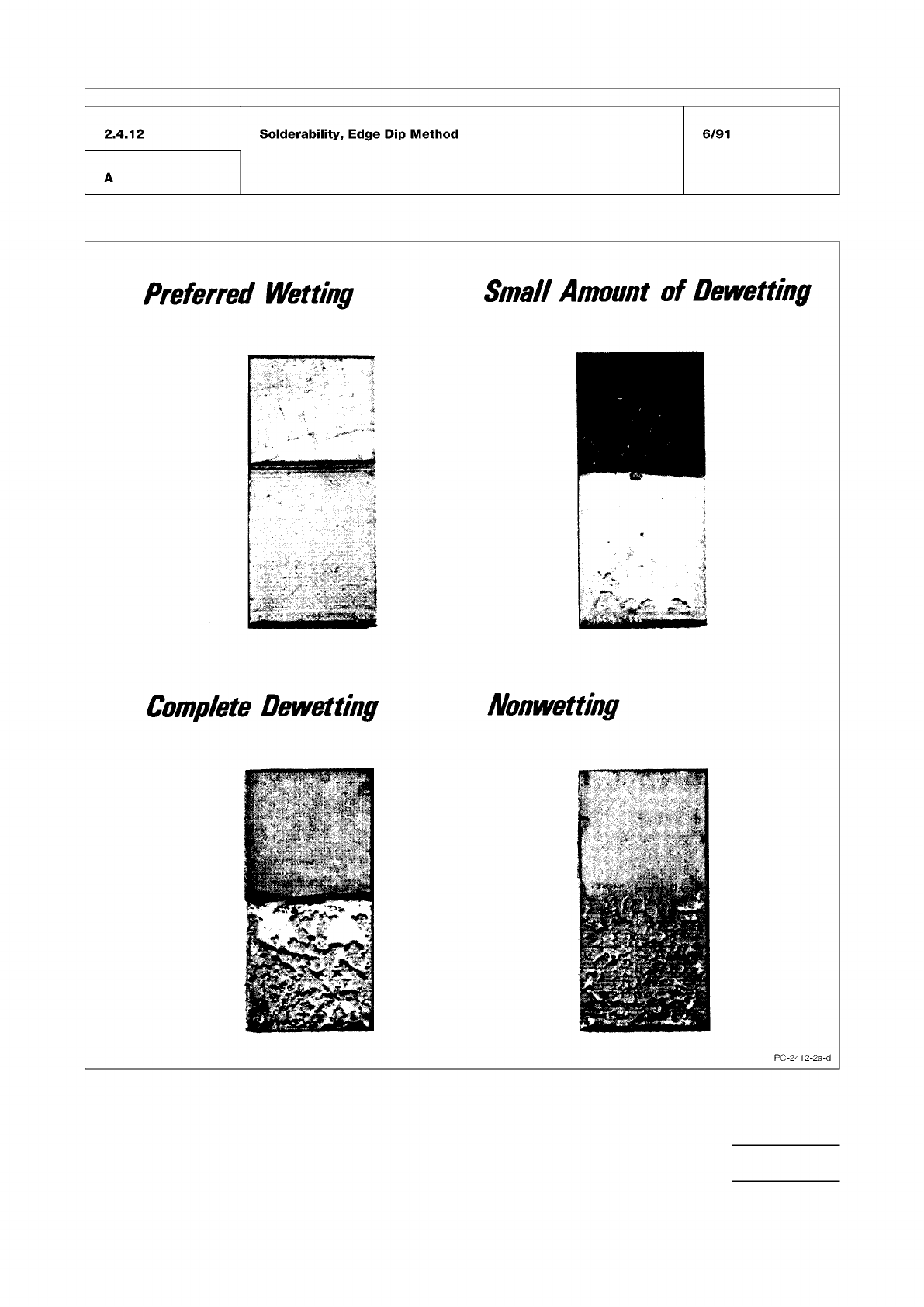
Figure 2 Aid to Evaluation
IPC-TM-650
Number
Subject Date
Revision
Page 3 of 3
Solderability,
Edge
Dip
Method
2.4.12
6/91
J-STD-004
Table 1 Solder Float Temperatures
Figure 1 Solder float test fixture
The Institute for Interconnecting and Packaging Electronic Circuits
2215 Sanders Road • Northbrook, IL 60062-6135
Material in this Test Methods Manual was voluntarily established by Technical Committees of the IPC. This material is advisory only
and its use or adaptation is entirely voluntary. IPC disclaims all liability of any kind as to the use, application, or adaptation of this
material. Users are also wholly responsible for protecting themselves against all claims or liabilities for patent infringement.
Equipment referenced is for the convenience of the user and does not imply endorsement by the IPC.
Page 1 of 1
IPC-TM-650
TEST
METHODS
MANUAL
1
Scope
This
test
method
establishes
and
defines
the
pro¬
cedures
for
determining
the
solder
float
resistance
of
copper
foil
clad
and
bare
flexible
dielectric
material.
2
Applicable
Documents
Requirements
for
Soldering
Fluxes
3
Test
Specimen
3.1
Two
specimens,
approximately
50
mm
x
50
mm
per
clad
side.
3.2
For
double
clad
laminate,
a
separate
specimen
unit
shall
be
prepared
and
tested
for
each
side.
The
copper
foil
shall
be
etched
from
the
reverse
or
nontest
side
of
each
specimen
using
standard
commercial
practices.
Bare
dielectric
material
shall
be
tested
bare.
4
Apparatus
4.1
Test
Chamber
A
circulating
air
chamber
capable
of
maintaining
a
uniform
temperature
of
135℃
±
10℃.
4.2
Solder
Pot
An
electrically-heated,
thermostatically-
controlled
solder
pot
of
adequate
dimensions
to
accommo¬
date
the
specimen
and
containing
no
less
than
2.25
Kg
of
solder.
4.3
Cutter
template
and
cutter
to
prepare
approximately
50
mm
x
50
mm
specimens
of
copper
clad
dielectric
material.
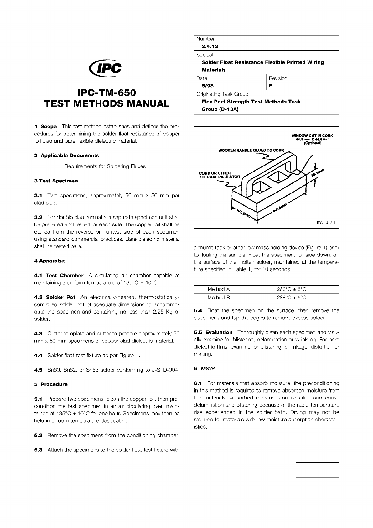
4.4
Solder
float
test
fixture
as
per
Figure
1
.
4.5
Sn60, Sn62,
or
Sn63
solder
conforming
to
J
-STD-004.
5
Procedure
5.1
Prepare
two
specimens,
clean
the
copper
foil,
then
pre¬
condition
the
test
specimen
in
an
air
circulating
oven
main¬
tained
at
135℃
±
10℃
for
one
hour.
Specimens
may
then
be
held
in
a
room
temperature
desiccator.
5.2
Remove
the
specimens
from
the
conditioning
chamber.
5.3
Attach
the
specimens
to
the
solder
float
test
fixture
with
Number
2.4.13
Subject
Solder
Float
Resistance
Flexible
Printed
Wiring
Materials
Date
Revision
5/98
F
Originating
Task
Group
Flex
Peel
Strength
Test
Methods
Task
Group
(D-13A)
a
thumb
tack
or
other
low
mass
holding
device
(Figure
1)
prior
to
floating
the
sample.
Float
the
specimen,
foil
side
down,
on
the
surface
of
the
molten
solder,
maintained
at
the
tempera¬
ture
specified
in
Table
1
,
for
1
0
seconds.
Method
A
260℃
土
5
℃
Method
B
288℃
±
5
℃
5.4
Float
the
specimen
on
the
surface,
then
remove
the
specimens
and
tap
the
edges
to
remove
excess
solder.
5.5
Evaluation
Thoroughly
clean
each
specimen
and
visu¬
ally
examine
for
blistering,
delamination
or
wrinkling.
For
bare
dielectric
films,
examine
for
blistering,
shrinkage,
distortion
or
melting.
6
Notes
6.1
For
materials
that
absorb
moisture,
the
preconditioning
in
this
method
is
required
to
remove
absorbed
moisture
from
the
materials.
Absorbed
moisture
can
volatilize
and
cause
delamination
and
blistering
because
of
the
rapid
temperature
rise
experienced
in
the
solder
bath.
Drying
may
not
be
required
for
materials
with
low
moisture
absorption
character¬
istics.