IPC-TM-650 EN 2022 试验方法--.pdf - 第309页
Figure 1 Suggested Dipping Device IPC-TM-650 Number Subject Date Revision Page 2 of 2 5.3.1 Clean the metal clad specimen by light abrasion or other suitable method, then flux the metal surface with a rosin flux conformi…
IPC-TM-650
MIL-F-14256
The Institute for Interconnecting and Packaging Electronic Circuits
2215 Sanders Road • Northbrook, IL 60062-6135
Material in this Test Methods Manual was voluntarily established by Technical Committees of the IPC. This material is advisory only
and its use or adaptation is entirely voluntary. IPC disclaims all liability of any kind as to the use, application, or adaptation of this
material. Users are also wholly responsible for protecting themselves against all claims or liabilities for patent infringement.
Equipment referenced is for the convenience of the user and does not imply endorsement by the IPC.
Page 1 of 2
IPC-TM-650
TEST
METHODS
MANUAL
1
Scope
This
test
method
is
used
to
determine
the
resis¬
tance
of
laminate
materials
(both
unclad
and
etched
surfaces)
to
the
thermal
abuse
of
a
solder
dip.
Resistance
to
softening,
loss
of
surface
resin,
scorching,
delamination,
blistering
and
measling
are
considered
in
the
evaluation.
2
Applicable
Documents
Test
Methods
Manual
2.4.1
Adhesion,
Tape
Testing
2.4.12
Solderability,
Edge
Dip
Method
Flux
3
Test
Specimen
Each
specimen
must
be
3.18
cm
x
3.18
cm
thickness.
A
separate
specimen
is
required
for
the
unclad,
etched,
fluxed,
and
unfluxed
tests.
Three
samples
are
required
from
each
sheet.
4
Equipment/Apparatus
4.1
An
electrically
heated,
thermostatically
controlled
pot
of
sufficient
size
to
accommodate
the
specimen
and
containing
no
less
than
2.25
kg
of
Sn6O
or
Sn63
4.2
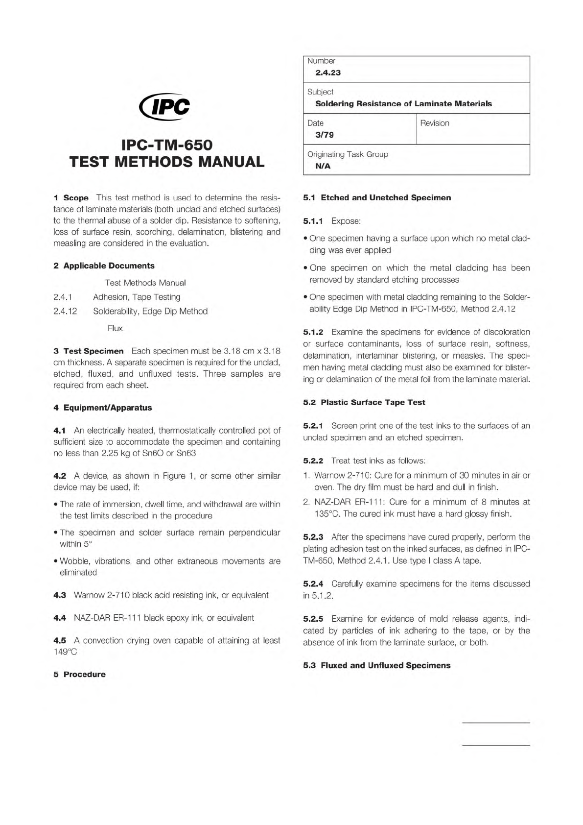
A
device,
as
shown
in
Figure
1
,
or
some
other
similar
device
may
be
used,
if:
•
The
rate
of
immersion,
dwell
time,
and
withdrawal
are
within
the
test
limits
described
in
the
procedure
•
The
specimen
and
solder
surface
remain
perpendicular
within
5
。
•
Wobble,
vibrations,
and
other
extraneous
movements
are
eliminated
4.3
Warnow
2-710
black
acid
resisting
ink,
or
equivalent
4.4
NAZ-
DAR
ER-1
1
1
black
epoxy
ink,
or
equivalent
4.5
A
convection
drying
oven
capable
of
attaining
at
least
149℃
Number
2.4.23
Subject
Soldering
Resistance
of
Laminate
Materials
Date
3/79
Revision
Originating
Task
Group
N/A
5.1
Etched
and
Unetched
Specimen
5.1.1
Expose:
•
One
specimen
having
a
surface
upon
which
no
metal
clad¬
ding
was
ever
applied
•
One
specimen
on
which
the
metal
cladding
has
been
removed
by
standard
etching
processes
•
One
specimen
with
metal
cladding
remaining
to
the
Solder¬
ability
Edge
Dip
Method
in
IPC-TM-650,
Method
2.4.12
5.1.2
Examine
the
specimens
for
evidence
of
discoloration
or
surface
contaminants,
loss
of
surface
resin,
softness,
delamination,
interlaminar
blistering,
or
measles.
The
speci¬
men
having
metal
cladding
must
also
be
examined
for
blister¬
ing
or
delamination
of
the
metal
foil
from
the
laminate
material.
5.2
Plastic
Surface
Tape
Test
5.2.1
Screen
print
one
of
the
test
inks
to
the
surfaces
of
an
unclad
specimen
and
an
etched
specimen.
5.2.2
Treat
test
inks
as
follows:
1
.
Warnow
2-710:
Cure
for
a
minimum
of
30
minutes
in
air
or
oven.
The
dry
film
must
be
hard
and
dull
in
finish.
2.
NAZ-
DAR
ER-1
11
:
Cure
for
a
minimum
of
8
minutes
at
135℃.
The
cured
ink
must
have
a
hard
glossy
finish.
5.2.3
After
the
specimens
have
cured
properly,
perform
the
plating
adhesion
test
on
the
inked
surfaces,
as
defined
in
IPC-
TM-650,
Method
2.4.1
.
Use
type
I
class
A
tape.
5.2.4
Carefully
examine
specimens
for
the
items
discussed
in
5.1.2.
5.2.5
Examine
for
evidence
of
mold
release
agents,
indi¬
cated
by
particles
of
ink
adhering
to
the
tape,
or
by
the
absence
of
ink
from
the
laminate
surface,
or
both.
5
Procedure
5.3
Fluxed
and
Unfluxed
Specimens
Figure 1 Suggested Dipping Device
IPC-TM-650
Number
Subject Date
Revision
Page 2 of 2
5.3.1
Clean
the
metal
clad
specimen
by
light
abrasion
or
other
suitable
method,
then
flux
the
metal
surface
with
a
rosin
flux
conforming
to
MIL-F-14256.
5.3.2
Clean
the
unclad
specimens
by
standard
production
techniques,
then
flux
the
laminate
material
with
a
rosin
flux
conforming
to
MIL-F-14256.
2.4.23
Soldering
Resistance
of
Laminate
Materials
3/79
5.3.3
Carefully
examine
all
specimens,
then
perform
the
tests
described
in
5.1.1
through
5.2.5.
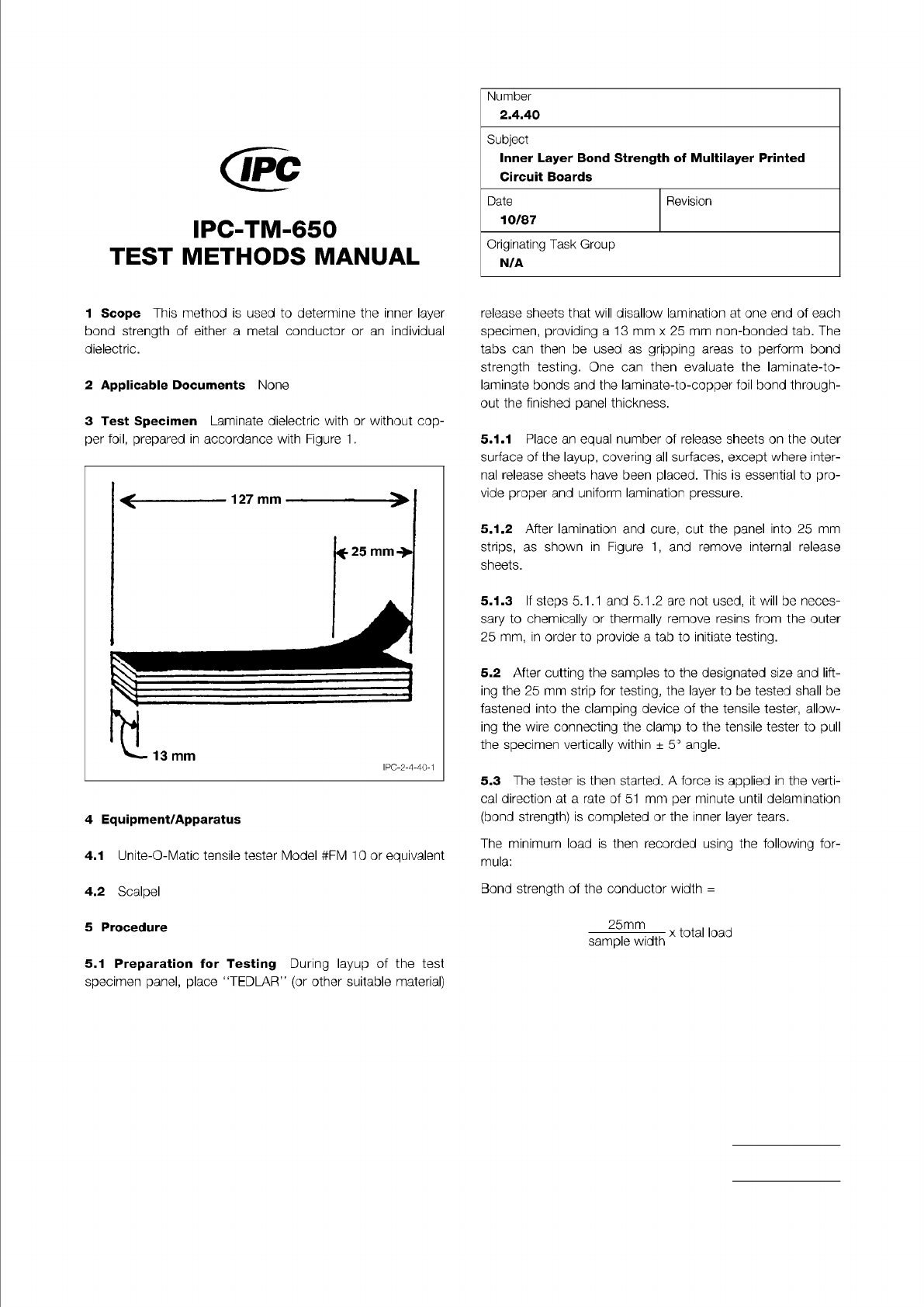
Figure 1 Laminate Dielectric
The Institute for Interconnecting and Packaging Electronic Circuits
2215 Sanders Road • Northbrook, IL 60062-6135
Material in this Test Methods Manual was voluntarily established by Technical Committees of the IPC. This material is advisory only
and its use or adaptation is entirely voluntary. IPC disclaims all liability of any kind as to the use, application, or adaptation of this
material. Users are also wholly responsible for protecting themselves against all claims or liabilities for patent infringement.
Equipment referenced is for the convenience of the user and does not imply endorsement by the IPC.
Page 1 of 1
IPC-TM-650
TEST
METHODS
MANUAL
1
Scope
This
method
is
used
to
determine
the
inner
layer
bond
strength
of
either
a
metal
conductor
or
an
individual
dielectric.
2
Applicable
Documents
None
3
Test
Specimen
Laminate
dielectric
with
or
without
cop¬
per
foil,
prepared
in
accordance
with
Figure
1
.
4
Equipment/Apparatus
4.1
Unite-O-Matic
tensile
tester
Model
#FM
10
or
equivalent
4.2
Scalpel
5
Procedure
Number
2.4.40
Subject
Inner
Layer
Bond
Strength
of
Multilayer
Printed
Circuit
Boards
Date
Revision
10/87
Originating
Task
Group
N/A
release
sheets
that
will
disallow
lamination
at
one
end
of
each
specimen,
providing
a
13
mm
x
25
mm
non-bonded
tab.
The
tabs
can
then
be
used
as
gripping
areas
to
perform
bond
strength
testing.
One
can
then
evaluate
the
laminate-to-
laminate
bonds
and
the
laminate-to-copper
foil
bond
through¬
out
the
finished
panel
thickness.
5.1.1
Place
an
equal
number
of
release
sheets
on
the
outer
surface
of
the
layup,
covering
all
surfaces,
except
where
inter¬
nal
release
sheets
have
been
placed.
This
is
essential
to
pro¬
vide
proper
and
uniform
lamination
pressure.
5.1.2
After
lamination
and
cure,
cut
the
panel
into
25
mm
strips,
as
shown
in
Figure
1
,
and
remove
internal
release
sheets.
5.1.3
If
steps
5.1.1
and
5.1
.2
are
not
used,
it
will
be
neces¬
sary
to
chemically
or
thermally
remove
resins
from
the
outer
25
mm,
in
order
to
provide
a
tab
to
initiate
testing.
5.2
After
cutting
the
samples
to
the
designated
size
and
lift¬
ing
the
25
mm
strip
for
testing,
the
layer
to
be
tested
shall
be
fastened
into
the
clamping
device
of
the
tensile
tester,
allow¬
ing
the
wire
connecting
the
clamp
to
the
tensile
tester
to
pull
the
specimen
vertically
within
±
5°
angle.
5.3
The
tester
is
then
started.
A
force
is
applied
in
the
verti¬
cal
direction
at
a
rate
of
51
mm
per
minute
until
delamination
(bond
strength)
is
completed
or
the
inner
layer
tears.
The
minimum
load
is
then
recorded
using
the
following
for¬
mula:
Bond
strength
of
the
conductor
width
二
25mm
sample
width
x
total
load
5.1
Preparation
for
Testing
During
layup
of
the
test
specimen
panel,
place
llTEDLAR"
(or
other
suitable
material)