IPC-TM-650 EN 2022 试验方法--.pdf - 第350页
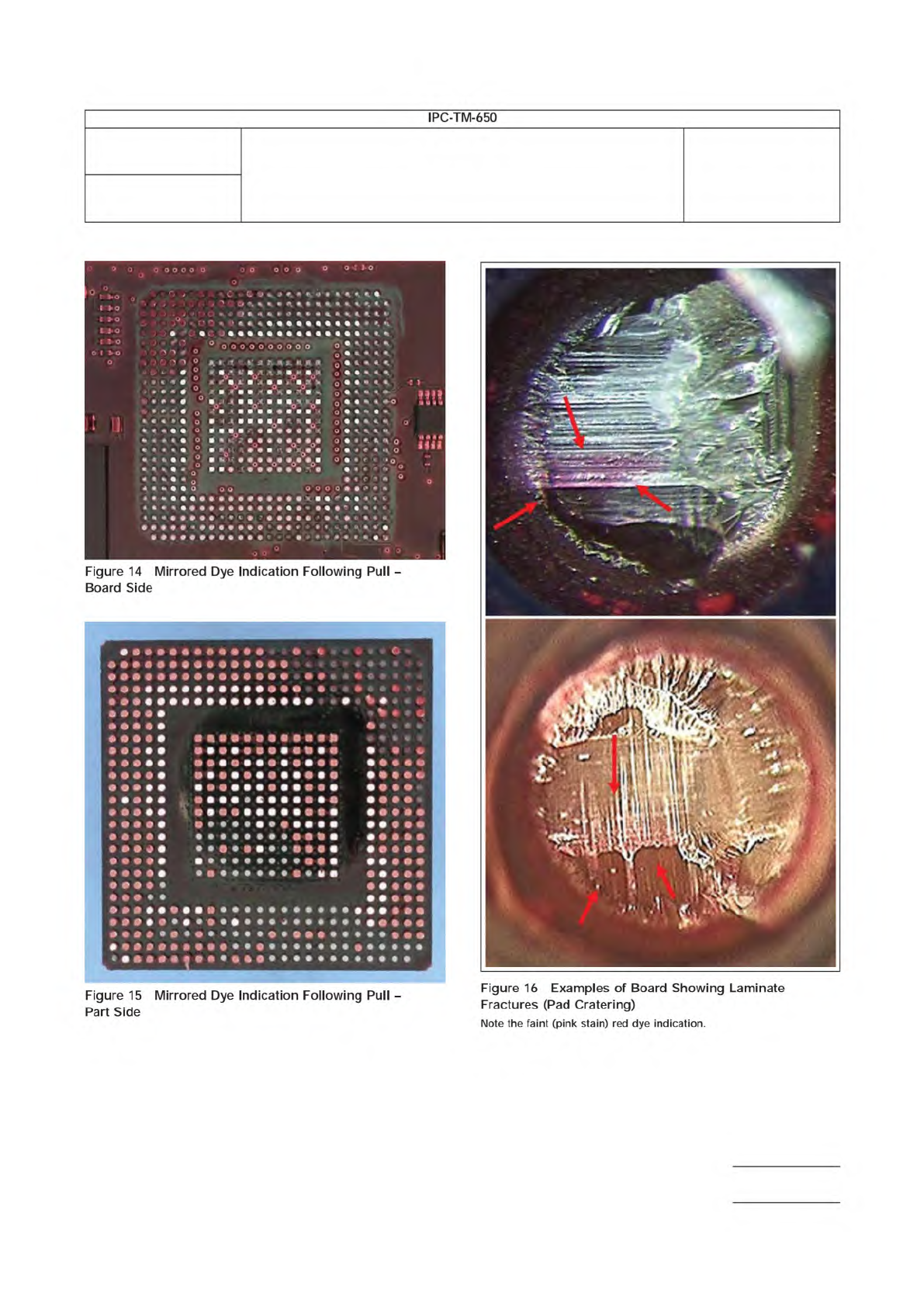
Number 2.4.53 Subject Dye and Pull Test Method (Formerly Known as Dye and Pry) Date 8/2017 Revision Page 7 of 1 1 Figure 14 Mirrored Dye Indication Following Pull - Board Side Figure 15 Mirrored Dye Indication Following …
Table 1 Test Report on Solder Paste
Enter appropriate information in top portion of report and complete report by entering the test results or checkmarks in the appropriate spaces.
Inspection Purpose: QPL I.D. Number:
__ Qualification Manufacturer’s Identification:
__ Quality Conformance A Manufacturer’s Batch Number:
__ Quality Conformance B Date of Manufacture:
__ Shelf-Life Extension Original Use-By Date:
__ Performance Revised Use-By Date:
Date Inspection Completed: Overall Results: __ Pass __ Fail
Inspection Performed by:
Witnessed by:
Inspections
User’s Actual
Requirement Test Result P/F (*) Tested by & Date
Material
Visual
Metal Content
Viscosity
Solder Ball
Slump
Alloy
Flux
Powder Size
% In Top Screen
% In Next Screen
% In Bottom Screen
% In Receiver Bottom
Max. Powder Size
Powder Shape
Tack
Wetting
* P/F = PASS/FAIL; enter P if test results are within tolerance of actual requirement; otherwise, enter F
IPC-TM-650
Number
Subject Date
Revision
Page 2 of 2
2.4.34.3
Solder
Paste
Viscosity
—
Spiral
Pump
Method
(Applicable
at
Less
Than
300,000
Centipoise)
1/95
Number
2.4.53
Subject
Dye and Pull Test Method (Formerly Known as Dye and Pry)
Date
8/2017
Revision
Page 7 of 11
Figure
14
Mirrored
Dye
Indication
Following
Pull
-
Board
Side
Figure
15
Mirrored
Dye
Indication
Following
Pull
-
Part
Side
Figure
16
Examples
of
Board
Showing
Laminate
Fractures
(Pad
Cratering)
Note
the
faint
(pink
stain)
red
dye
indication.
IPC-TM-650
—
1 2
A
B
C
D
IPC-2-4-53-19
1
2
5
3
6
7
9
8
10
4
Number
2.4.53
Subject
Dye and Pull Test Method (Formerly Known as Dye and Pry)
Date
8/2017
Revision
Page 8 of 11
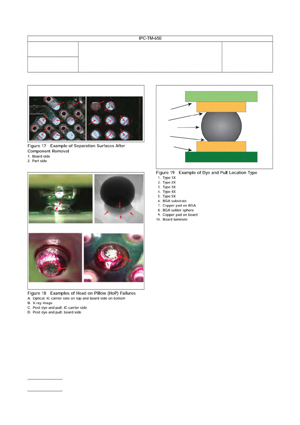
Figure
17
Example
of
Separation
Surfaces
After
Component
Removal
1.
Board
side
2.
Part
side
Figure
19
Example
of
Dye
and
Pull
Location
Type
2
3
4
5
6
BGA
substrate
7
8
9
10
Copper
pad
on
BGA
BGA
solder
sphere
Copper
pad
on
board
Board
laminate
Figure
18
Examples
of
Head
on
Pillow
(HoP)
Failures
A.
Optical;
IC
carrier
side
on
top
and
board
side
on
bottom
B.
X-ray
image
C.
Post
dye
and
pull;
IC
carrier
side
D.
Post
dye
and
pull;
board
side
IPC-TM-650
—
X
X
X
X
X
1
2
3
4
5
e
e
e
e
e
p
p
p
p
p