IPC-TM-650 EN 2022 试验方法--.pdf - 第410页
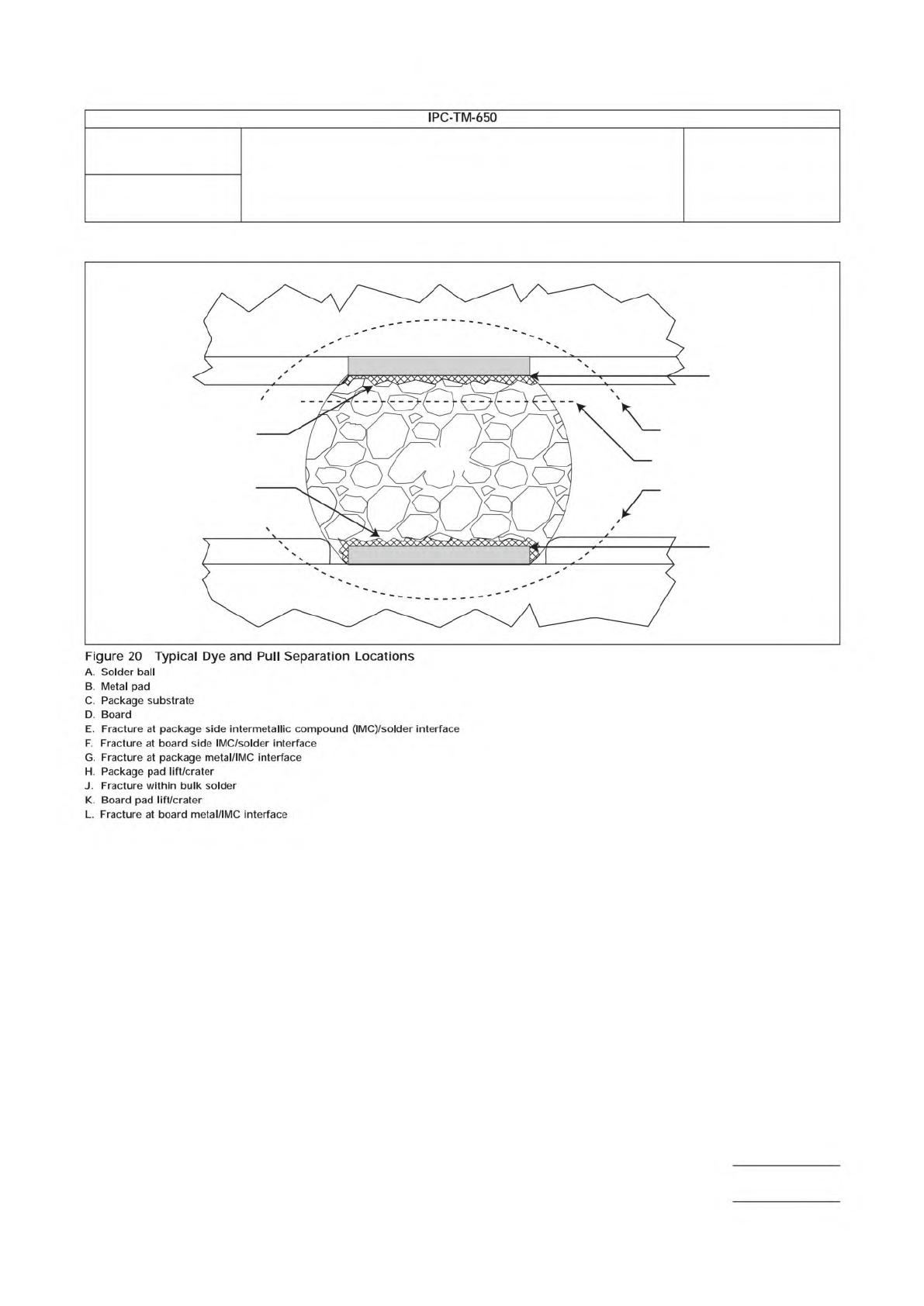
IPC-2-4-53-20 A B C D E F G H J K L B Number 2.4.53 Subject Dye and Pull Test Method (Formerly Known as Dye and Pry) Date 8/2017 Revision Page 9 of 1 1 IPC-TM-650 Figure 20 Typical Dye and Pull Separation Locations A. So…
1 2
A
B
C
D
IPC-2-4-53-19
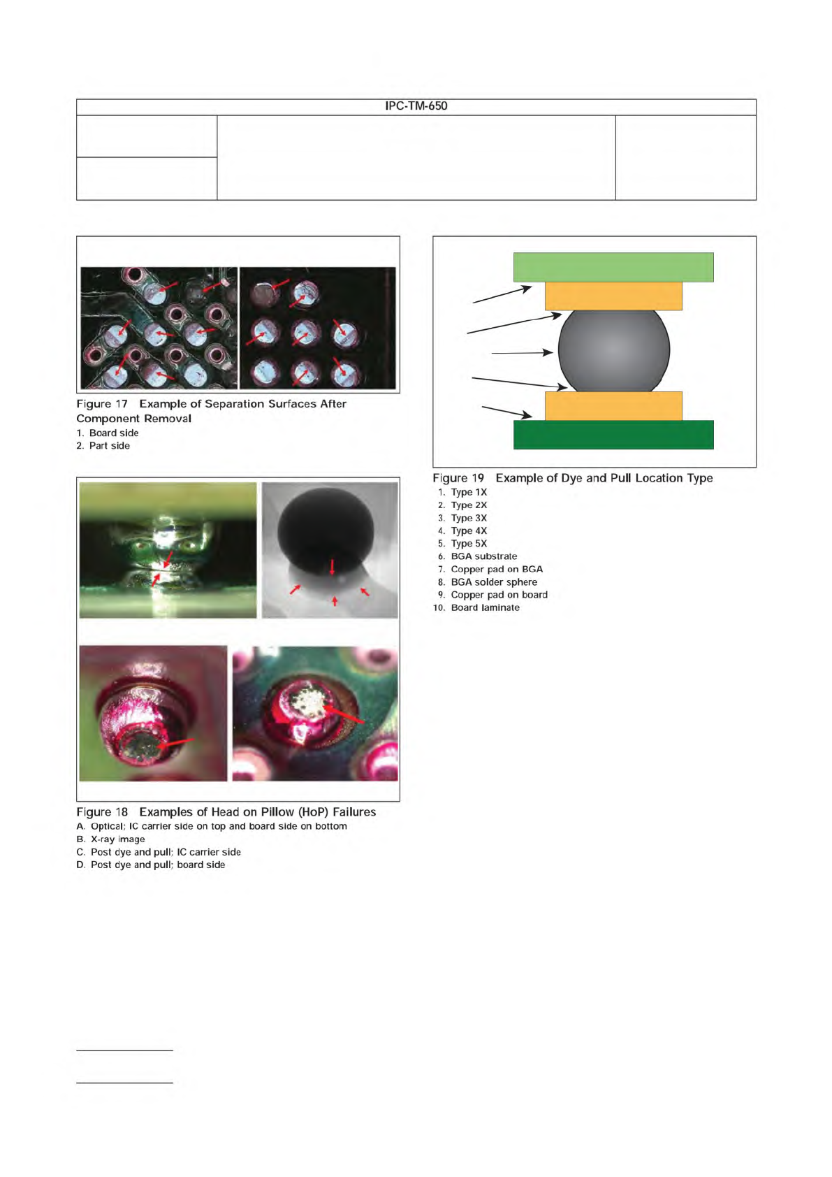
1
2
5
3
6
7
9
8
10
4
Number
2.4.53
Subject
Dye and Pull Test Method (Formerly Known as Dye and Pry)
Date
8/2017
Revision
Page 8 of 11
Figure
17
Example
of
Separation
Surfaces
After
Component
Removal
1.
Board
side
2.
Part
side
Figure
19
Example
of
Dye
and
Pull
Location
Type
2
3
4
5
6
BGA
substrate
7
8
9
10
Copper
pad
on
BGA
BGA
solder
sphere
Copper
pad
on
board
Board
laminate
Figure
18
Examples
of
Head
on
Pillow
(HoP)
Failures
A.
Optical;
IC
carrier
side
on
top
and
board
side
on
bottom
B.
X-ray
image
C.
Post
dye
and
pull;
IC
carrier
side
D.
Post
dye
and
pull;
board
side
IPC-TM-650
—
X
X
X
X
X
1
2
3
4
5
e
e
e
e
e
p
p
p
p
p
IPC-2-4-53-20
A
B
C
D
E
F
G
H
J
K
L
B
Number
2.4.53
Subject
Dye and Pull Test Method (Formerly Known as Dye and Pry)
Date
8/2017
Revision
Page 9 of 11
IPC-TM-650
Figure
20
Typical
Dye
and
Pull
Separation
Locations
A.
Solder
ball
B.
Metal
pad
C.
Package
substrate
D.
Board
E.
Fracture
at
package
side
intermetallic
compound
(IMC)/solder
interface
F.
Fracture
at
board
side
IMC/solder
interface
G.
Fracture
at
package
metal/IMC
interface
H.
Package
pad
lift/crater
J.
Fracture
within
bulk
solder
K.
Board
pad
lift/crater
L.
Fracture
at
board
metal/IMC
interface
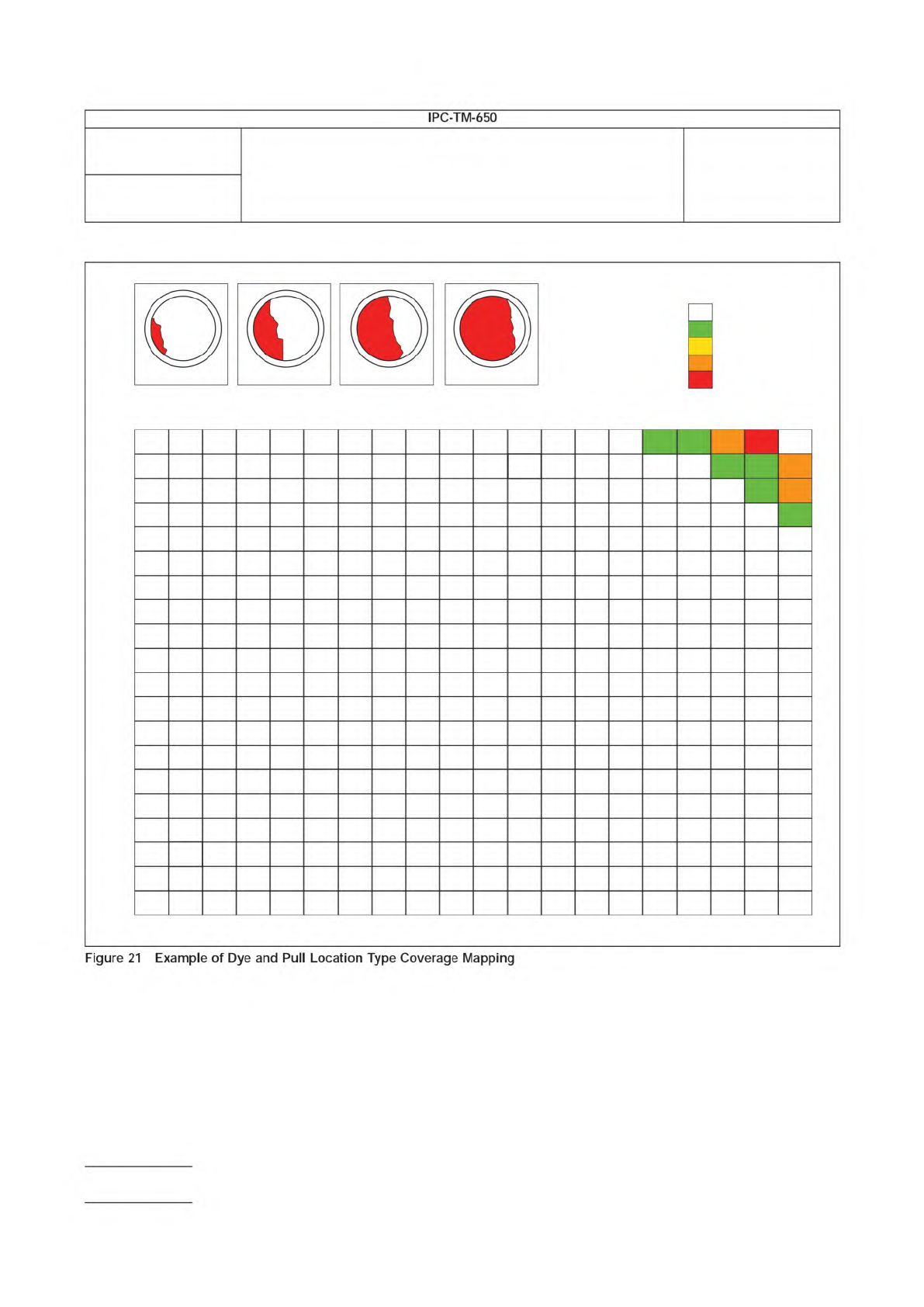
IPC-2-4-53-21
B
A
= 0 %
= 1 to 25 %
= 26 to 50 %
= 51 to 75 %
= 76 to 100 %
B
C
D
E
C D E
1
A X
X X
X
B
C
D
E
F
G
H
J
K
L
M
N
O
P
Q
R
T
U
V
W
2 3 4 5 6 7 8 9 10 11 12 13
2B 4B 3D
3D
2D
3E
3B
3B
2B
2B
14 15 16 17 18 19 20
Number
2.4.53
Subject
Dye and Pull Test Method (Formerly Known as Dye and Pry)
Date
8/2017
Revision
Page 10 of 11
IPC-TM-650
―
Figure
21
Example
of
Dye
and
Pull
Location
Type
Coverage
Mapping