IPC-TM-650 EN 2022 试验方法--.pdf - 第413页
Number Subject Date Revision Originating T ask Gr oup MaterialinthisT estM ethodsManualwasvoluntarilyestablis hedby T echnicalCommitteesofIPC.Thismaterialisadvisoryonly anditsuseoradaptationisen…
IPC-2-4-53-22
1
A
a
b
B
C
D
E
F
G
H
J
K
L
M
N
O
P
Q
R
T
U
V
W
2 3 4 5 6 7 8 9 10 11 12 13 14 15 16 17 18 19 20
Number
2.4.53
Subject
Dye and Pull Test Method (Formerly Known as Dye and Pry)
Date
8/2017
Revision
Page 11 of 11
IPC-TM-650
—
Complete
dye
indication
Partial
dye
indication
Partial
dye
indication
at
two
interfaces
Complete
dye
indications
at
two
interfaces
Partial
and
complete
dye
indication
at
two
interfaces
No
dye
indication
Separation
between
board
laminate
and
board
pad
Separation
between
solder
and
board
pad
Separation
through
solder
joint
Separation
between
solder
and
component
pad
Separation
between
component
substrate
and
component
pad
Other
=
Double
separation
between
board
laminate/board
pad
and
solder/board
pad
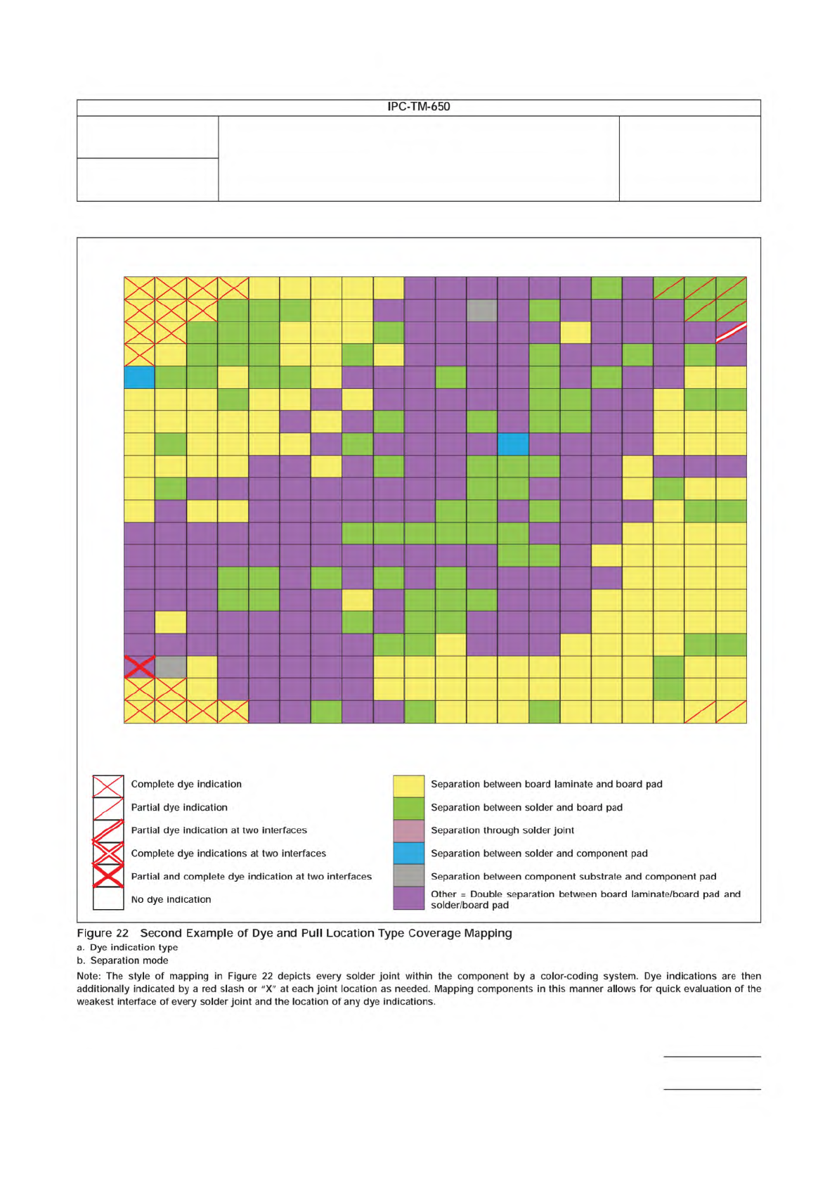
Figure
22
Second
Example
of
Dye
and
Pull
Location
Type
Coverage
Mapping
a.
Dye
indication
type
b.
Separation
mode
Note:
The
style
of
mapping
in
Figure
22
depicts
every
solder
joint
within
the
component
by
a
color-coding
system.
Dye
indications
are
then
additionally
indicated
by
a
red
slash
or
"X"
at
each
joint
location
as
needed.
Mapping
components
in
this
manner
allows
for
quick
evaluation
of
the
weakest
interface
of
every
solder
joint
and
the
location
of
any
dye
indications.

Number
Subject
Date Revision
Originating Task Group
MaterialinthisTestMethodsManualwasvoluntarilyestablishedbyTechnicalCommitteesofIPC.Thismaterialisadvisoryonly
anditsuseoradaptationisentirelyvoluntary.IPCdisclaimsallliabilityofanykindastotheuse,application,oradaptationofthis
material.Usersarealsowhollyresponsibleforprotectingthemselvesagainstallclaimsorliabilitiesforpatientinfringement.
EquipmentreferencedisfortheconvenienceoftheuseranddoesnotimplyendorsementbyIPC.
3000 Lakeside Drive, Suite 105 N
Bannockburn, Illinois 60015-1249
IPC-TM-650
TEST METHODS MANUAL
Page 1 of 7
2.4.54
09/2022 N/A
D-33AAIPC-6012AutomotiveAddendumTaskGroup
TestMethodforThermalTransmissionPropertiesof
MetalBasedPrintedBoards(MBPB)
1 Scope
1.1
The scope of the test method is to describe a procedure for measurement of thermal resistance and calculation of an apparent
thermal conductivity for single layer Metal Based Printed Boards (MBPB). This test method has been created to address the
issue of measurement uncertainty for materials with low thermal resistance (high thermal conductivity and/or thin thicknesses).
1.2
Precise measured values of thermal resistance are very important, for multiple applications, especially within automotive
sector, but also in other areas. For materials with a low thermal resistance, the measurement uncertainty increases significantly
when using the steady state measuring method. The target for this test method is to provide good repeatability and reproducibility
in the test result. A certified reference material must be used to guarantee the measurement quality.
The test method shall show a validity of different thermal resistance values represented by different thicknesses and materials
used for the MBPB. The test method shall also describe a reliable thickness measurement.
1.3 Terms and Definitions
Other than those terms listed below, the definitions of terms used in this test method are in accordance
with IPC-T-50.
1.3.1 Thermal Conductivity
Thermalconductivityapplies inthis caseto the bulk valueofthe metallayers(λ
base
orλ
top
see
Table1Equations12and13)orthealuminumbarsforhotorcoldside(λ
h
orλ
c
see Table 1 Equations 1 and 2) and the dielectric
materialfilledwithoxideparticlesofdifferentkindoffillerdegree(λ
die
) (Figure 5).
1.3.2 Apparent Thermal Conductivity
Apparent thermal conductivity includes the bulk thermal conductivity of the dielectric
material filled with oxide particles, the treatment or adhesive layer and the thermal contact resistances (see 1.3.5) to the upper
andlowermetallayers(λ
app.,die
see Table 1 Equation 16).
1.3.3 Total Thermal Resistance
Total thermal resistance R
th,total
applies to the measured thermal resistance of the MBPB and the
contact liquid (R
th,total
see Table 1 Equation 10).
1.3.4 Apparent Thermal Resistance Specimen
Apparent thermal resistance specimen R
th, app,specimen
applies to the measured thermal
resistance of the MBPB. This has an upper and lower metal layer. In-between it has a dielectric layer with the two contact
resistances to the metal layers (R
th, app,specimen
see Table 1 Equation 11).
1.3.5 Thermal Contact Resistance
Thermal contact resistance applies to a contact phenomenon between two bodies. A contact
resistance can arise due to suboptimal surface wetting, high surface roughness or influenced heat flow density at the boundary
layer due to the following parameters: the filler concentration, particle percolation path, particle distribution and particle size.
This contact resistance leads to a variance in measurement results.
1.3.6 Surface Area
Surface area is calculated from the diameter of the meter bars in the dimension mm².
1.4
Technical safety requirements are not defined in this test method. The user must take measures to fulfil all statutory health,
safety and environmental protection requirements.
BUILD
ELECTRONICS
BETTER

IPC-TM-650
Number Subject Date
Revision
Page 2 of 7
2.4.54
TestMethodforThermalTransmissionPropertiesof
09/2022
MetalBasedPrintedBoards(MBPB)
N/A
2 Applicable Documents
2.1 IPC Documents
1
IPC-4101C
Specification for Base Materials for Rigid and Multilayer Printed Boards
IPC-TM-650
Test Methods Manual
2.1.1 Microsectioning, Manual and Semi or Automatic
2.1.1.2 Microsectioning—Semi or Automatic Technique Microsection Equipment
2.2 International Organization of Legal Metrology
2
OIMLG14
Density measurement
2.3 ASTM
3
ASTME1461
Standard Test Method for Thermal Diffusivity by the Flash Method
ASTME1269
Standard Test Method for Determining Specific Heat Capacity by Differential Scanning Calorimetry
3 Test Specimens
3.1
The sample thickness can be measured within the machine or before and after measurement. In both cases the accuracy
should be smaller than 10 µm.
3.2
Prepare specimens from its original, treated or aged condition. Clean the surfaces from any kind of dirt. The solvents
have to be chosen carefully as possible adverse reactions with the surface of the sample could occur (see IPC-TM-650
Test Method 2.1.1).
3.3
The specimen has to be manufactured e.g., by milling or other kind of processing. Remove burrs and flashes on the edge
of the specimen.
3.4
Create three specimens from one raw laminate panel. Ensure a distance from the border of about 50 mm to avoid tolerance
deviations of the dielectric material.
3.5
Ensure that the surface of the specimen is free of scratches, waviness or any kind of damage. Photos should be included
into the test report.
4 Apparatus or Material
4.1
Figures 1 and 3 shows parts for an apparatus, which fulfills the requirements for this test method.
4.2
Ensure that the surfaces of the aluminum bars are free from scratches or other damages. The surface has to be smooth
(Ra≤1µm).
4.3
Use a method to measure the total thickness of the specimen like contactless with laser, LED detector or before and after
measurement with a micrometer screw according to IPC-4101C.
4.4
Use insulated heat flow meter bars on both sides, hot and cold in order to prevent heat losses to the environment and thus
improve the measurement accuracy.
4.5
Due to the forced heat flow, the apparatus needs both a heat as well as a cooling source. There are several options for
heating and cooling. The recommended method of heating is the usage of an electrical heater which is embedded in a copper
block. Other options can be liquid heaters. Regardless of the method. It is important to use constant temperatures at heat and
cooling side.
4.6
The heat flow meter bars of the apparatus need to be constructed out of well-known and thermally characterized (see
ASTM E1461 for thermal diffusivity, ASTM E1269 for specific heat capacity, and OIML G 14 for density) material in the
1 www.ipc.org
2 www.oiml.org
3 www.astm.org
―