IPC-TM-650 EN 2022 试验方法--.pdf - 第427页
The Institute for Int erconnecting and Packaging E lectronic Circuits 2215 Sanders Road • Northbrook, IL 60062 Material in this T est M ethods Manual was vol untaril y establis hed by T echni cal Committees of the IP C. …

mechanical probing methods. Operators and probing equip-
ment should be tested in ability to repeat electrical probe con-
tacts.
6.3.6.1 Probes for Single-Ended Transmission Line
Measurements
The probe assembly impedance is often
chosen to be 50 Ω to match the impedance of the TDR sys-
tem. Impedance matching minimizes reflections at the inter-
face between the probe and the transmission line under test.
These reflections, which appear at and around the transition
region in the TDR pulse and can extend for some time after
this transition, are perturbations in the TDR waveform and are
undesirable because they may affect the computation of the
reference level instant, thereby increasing measurement
uncertainty. When the characteristic impedance of the trans-
mission line under test is nominally 50 Ω, these perturbations
will normally decay rapidly. If the impedance of the transmis-
sion line under test is significantly different from 50 Ω, the
magnitude of the perturbations can be large and their duration
long enough to affect the computation of the reference level
instant. The effect of these perturbations must be taken into
account when determining the appropriate waveform epoch
(see 4.1.2). The design and quality of manufacture of the
probe has a large effect on the magnitude and duration of
reflections generated between the TDR system and the trans-
mission line under test.
When probing non-50 Ω lines, it is possible to separate, in the
TDR waveform, the large signal perturbations caused by the
TDR/probe interface from those caused by the probe/
transmission line interface. To do this, a specially designed
probe is required that is impedance matched to the transmis-
sion line under test and that also has a long propagation delay
between the TDR/probe connection and the probe tip. The
long propagation delay can effectively move the large pertur-
bations at the TDR/probe interface out of the waveform
epoch.
6.3.6.2 Probes for Coupled-Signal-Line (Differential)
Transmission Line Measurements
The probe consider-
ations described in 4.3.3 apply for probes used in differential
transmission line measurements. However, the necessity to
simultaneously probe two signal lines and one or two refer-
ence plane contacts makes differential probing more difficult
than probing single signal line structures. In a PB manufactur-
ing environment, the use of two probes that were previously
used for single-ended measurements may not be possible.
This is because the operator is required to use both hands for
probing, which leaves them unable to operate the instrument.
Contact your instrument manufacturer for their probing solu-
tions and advice. Probes from one manufacturer can also be
used with another manufacturer’s TDR if the impedance val-
ues and connectors are compatible.
6.4 Adjustable Measurement Parameters
6.4.1 Sampling Interval (Point Spacing)
The temporal
resolution of the TDR unit is an issue only if it affects the dura-
tion of the transitions in the TDR waveforms (see 4.1.2) that
are used to compute t
d
. The temporal resolution of the TDR is
affected by the transition duration of the TDR step response,
the transition duration of the step response of all intervening
electrical components (connectors, cables, adapters), mea-
surement jitter, the interval between sampling instances, and
timebase errors. For typical TDR measurements, timebase
errors and sampling intervals should not be an issue (both are
or can be made to be less than 10 ps). The effect of measure-
ment jitter can be modeled by convolving the jitter distribution
with the TDR step response to yield an effective TDR step
response. The effect of jitter on the bandwidth of the TDR
measurement can be assessed from the jitter spectrum,
which can be described by:
J(,) = e
−2(πσ,)
2
,
where
J is the jitter spectrum,
f is frequency, and
σ is the rms jitter value.
If the effective jitter step response differentially impacts the
duration of the two or more waveform transitions used to
compute t
d
, then jitter must be reduced. More than likely, jit-
ter will be nearly identically distributed for each transition. But
if the jitter is so great as to affect the accuracy of computing
the transition instants, then the user must reduce the duration
of the waveform period or reduce the system jitter. Reduction
in the duration of the waveform period may introduce a bias in
the voltage values and this may affect the computed value of
t
d
. If the rms jitter value is less than 20% of the transition
duration of the TDR step response, then the jitter is small and
can be ignored. For typical TDR systems, however, rms jitter
is less than 10 ps and will not affect the t
d
measurements.
Similarly, the effect of cables, connectors, and adapters on
the measurement can be modeled by convolving their step
responses with that of the TDR unit. If the transition duration
of this new step response meets the requirements of 4.1.2,
then the performance of the cables, connectors, and adapters
is adequate.
Number
2.5.5.11
Subject
Propagation Delay of Lines on Printed Boards by TDR
Date
04/2009
Revision
IPC-TM-650
Page
15
of
16
The Institute for Interconnecting and Packaging Electronic Circuits
2215 Sanders Road • Northbrook, IL 60062
Material in this Test Methods Manual was voluntarily established by Technical Committees of the IPC. This material is advisory only
and its use or adaptation is entirely voluntary. IPC disclaims all liability of any kind as to the use, application, or adaptation of this
material. Users are also wholly responsible for protecting themselves against all claims or liabilities for patent infringement.
Equipment referenced is for the convenience of the user and does not imply endorsement by the IPC.
Page 1 of 2
IPC-TM-650
TEST
METHODS
MANUAL
1
.0
Scope
This
test
method
is
to
determine
the
dielectric
constant
and
dissipation
factor
of
raw
printed
wiring
board
material
at
1
MH
乙
2
.0
Applicable
Documents
None
3
.0
Test
Specimens
Each
specimen
shall
be
50.8
±
0.076
mm
[2.0
±
0.003
in]
in
diameter
by
thickness
of
laminate
or
substrate
material.
Remove
copper
of
metal-clad
specimens
by
etching
using
standard
commercial
practices.
At
least
three
specimens
are
required.
4
.0
Equipment/Apparatus
4.1
Meter
A
1
MHz
Digital
LCR
Meter,
Hewlett
Packard
Mdl
4271
A
or
equivalent.
4.2
Test
Fixture
Hewlett
Packard
Mdl
1
6022A
test
fixture
or
equivalent.
4.3
Specimen
Holder
A
special
specimen
holder
made
as
shown
in
Figure
1.
This
holder
is
designed
to
be
compatible
with
the
H/P
test
fixture,
Mdl
1
6022A.
4.0
Procedure
5.1
Preparation
5.1.1
Prepare
the
specimens
as
specified
in
paragraph
3.0.
5.1.2
Calculate
the
effect
thickness
(inches)
=
0.01942
x
Mass
Density
Mass
=
Measured
weight
in
grams
Density
=
Grams
per
cubic
cm
(as
per
ASTM-D-792,
Method
1A)
5.1.3
Coat
both
sides
of
specimens
with
one
uniform
coat¬
ing
of
silver
conductive
paint.
5.1.4
Air-dry
the
specimens
until
dry
to
touch,
then
oven-dry
at
50°
±
2
℃
for
1
/2
hour
and
cool
in
a
desiccator.
Number
2.5.5.2
Subject
Dielectric
Constant
and
Dissipation
Factor
of
Printed
Wiring
Board
Material
—
Clip
Method
Date
Revision
12/87
A
Originating
Task
Group
N/A
5.1.5
Punch
or
machine
a
25.4
mm
[1
.0
in]
diameter
disc
from
the
50.8
mm
[2.0
in]
specimens.
(Assure
that
there
is
no
carry
over
of
the
paint
from
one
side
to
the
other.)
5.1.6
Condition
the
25.4
mm
[1
.0
in]
specimens
for
a
mini¬
mum
of
40
hours
at
23°
±
5
℃
at
a
relative
humidity
of
50%.
5.2
Testing
5.2.1
Turn
meter
on
and
allow
to
warm
up
for
60
minutes
minimum.
5.2.1.
1
Set
the
controls
on
the
meter
as
follows:
Function
-
C-D
Range
-
Manual
Trigger
-
Internal
Rate
-
FCW
Test
Signal
Level
-
Low
5.2.1.
2
Connect
the
cables
for
the
test
fixture
to
the
appro¬
priate
connectors.
5.2.2
Plug
the
special
specimen
holder
into
the
test
fixture.
5.2.3
The
digital
display
on
the
meter
will
show
the
capaci¬
tance
value
and
the
dissipation
factor
of
the
unknown
dielec¬
tric
specimen.
5.3
Calculation
5.3.1
Dielectric
Constant
The
dielectric
constant
shall
be
determined
by
using
the
following
formula:
K
=
―
—
—
0.225
A
K
=
Dielectric
constant
C
=
Capacitance
reading
from
Mdl
4271
A
Meter
A
=
Area
of
a
1
-inch
disc
(square
inches)
t
=
Effective
thickness
(inches)
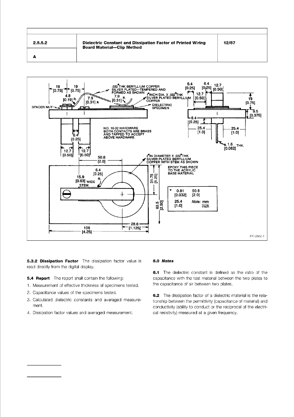
Figure 1 Special Test Fixture for Dielectric Constant and Dissipation Factor Measurements
IPC-TM-650
Number
Subject Date
Revision
Page 2 of 2
2.5.5.2
Dielectric
Constant
and
Dissipation
Factor
of
Printed
Wiring
Board
Material
—
Clip
Method
12/87
A
Q32,HK
BERYLLIUM
C
SILVER
PLATED—
TEMP
FORMED
AS
SHOWN
俞
7
融/
/
r
SPACER
N(
I
T
q
I
I
I
6.4
).2E
NO.
10-32
HARDWARE
BOTH
CONTACTS
ARE
BRAS
AND
TAPPED
TO
ACCEPT
ABOVE
HARDWARE.
K
•I
L-
12.7
[0.50]
K
C
12.7
[0.50]
50.8
2’
ys
Zc
卬
5
.
1
[0
6.4
一
[0.25]
/
5.9
r
/
•63]
WIDE
i/
y
STEM
Q
/
e
)
7
108
L25
—
[1.125]
—
r
k
J
r
COPPER
J
>ERED
AND
W
*INCH
DIA.
X
.032*THK
SILVER
PLATED
BERYLLIU
TOPPER
x
DIELECTRIC
SPECIMEN
5.4
.25
I
6
1
[0
12.7
[0.50]
.4
,
[2
7
巴哉。
11
tl~L
中
L
[0.
M
HO\
PIE
YLI
UAL
f
9.5
1
[0.375]
SS
力
N
DIA
SILVER
:
OPPEF
工
1
9
2
METER
X
.03
落
HK
'LATED
BERYLLIU
WITH
STEM
AS
S
EPOXY
THIS
TO
THE
ACR
BASE
MATEF
25]
丁
_25.4
—
[1.0)
WN
CE
二
1
1
阳
T
[01062]THK
I
*
0.81
50.8
[0.032]
[2.0]
&
|
25.4
Note:
mm
卷
I
[10]
麻
IPC-2552-1
5.3.2
Dissipation
Factor
The
dissipation
factor
value
is
read
directly
from
the
digital
display.
5.4
Report
The
report
shall
contain
the
following:
1
.
Measurement
of
effective
thickness
of
specimens
tested.
2.
Capacitance
values
of
the
specimens
tested.
3.
Calculated
dielectric
constants
and
averaged
measure¬
ment.
4.
Dissipation
factor
values
and
averaged
measurement.
6.0
Notes
6.1
The
dielectric
constant
is
defined
as
the
ratio
of
the
capacitance
with
the
test
material
between
the
two
plates
to
the
capacitance
of
air
between
two
plates.
6.2
The
dissipation
factor
of
a
dielectric
material
is
the
rela¬
tionship
between
the
permittivity
(capacitance
of
material)
and
conductivity
(ability
to
conduct
or
the
reciprocal
of
the
electri¬
cal
resistivity)
measured
at
a
given
frequency.