IPC-TM-650 EN 2022 试验方法--.pdf - 第433页
B. Gore, J. L oyer, R. Mellitz, M. Gaudion, J. Burnikell, P. Carre, ‘‘Towa rds a PB Production Floor Metric for Go/No Go Testing of Lo ssy High Speed Tran smission Lines,’’ from IPC Expo 2008. A. Deutsch, G . Arjavalinga…
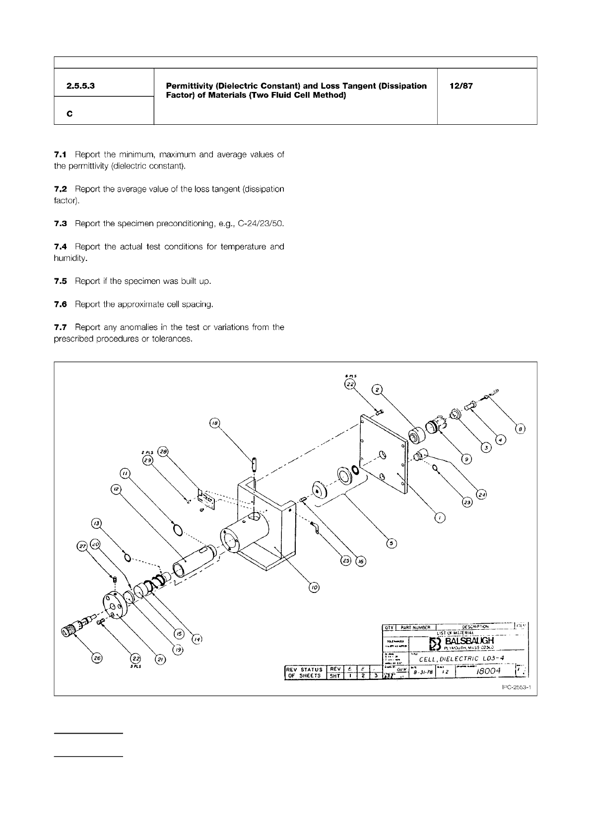
Figure 1
IPC-TM-650
Number
Subject Date
Revision
Page 4 of 4
12/87
2.5.5.3
Permittivity
(Dielectric
Constant)
and
Loss
Tangent
(Dissipation
Factor)
of
Materials
(Two
Fluid
Cell
Method)
7.1
Report
the
minimum,
maximum
and
average
values
of
the
permittivity
(dielectric
constant).
7.2
Report
the
average
value
of
the
loss
tangent
(dissipation
factor).
7.3
Report
the
specimen
preconditioning,
e.g.,
C-24/23/50.
7.4
Report
the
actual
test
conditions
for
temperature
and
humidity.
7.5
Report
if
the
specimen
was
built
up.
7.6
Report
the
approximate
cell
spacing.
7.7
Report
any
anomalies
in
the
test
or
variations
from
the
prescribed
procedures
or
tolerances.
B. Gore, J. Loyer, R. Mellitz, M. Gaudion, J. Burnikell, P.
Carre, ‘‘Towards a PB Production Floor Metric for Go/No Go
Testing of Lossy High Speed Transmission Lines,’’ from IPC
Expo 2008.
A. Deutsch, G. Arjavalingam, and G. Kopcsay, ‘‘Characteriza-
tion of Resistive Transmission Lines by Short Pulse Propaga-
tion,’’ in IEEE Microwave and Guided Wave Letters, vol. 2,
no.1, January 1992.
A. Deutsch, G. Arjavalingam, G. Kopcsay, and M. Deger-
strom, ‘‘Short-Pulse Propagation Technique for Characteriz-
ing Resistive Package Interconnections,’’ in IEEE Transactions
on Components, Hybrids, and Manufacturing Technology, vol.
15, no. 6, December 1992.
A. Deutsch, T. M. Winkel, G. Kopcsay, C. Surovic, B. Rubin,
G. Katopis, B. Chamberlin, R. Krabbenhoft, ‘‘Extraction of ε
r
(f)
and tanδ(f) for Printed Circuit Board Insulators Up to 30 GHz
Using the Short Pulse Propagation Technique’’ in IEEE Trans-
actions on Advanced Packaging, vol. 20, no. 1, February
2005.
A. Deutsch, C. W. Surovic, R. S. Krabbenhoft, G. V. Kopcsay,
B. J. Chamberlin, ‘‘Prediction of Losses Caused by Rough-
ness of Metallization in Printed-Circuit Boards,’’ IEEE Transac-
tions on Advanced Packaging, vol. 30, no.2, pp.279-287,
May 2007.
A. Deutsch, Roger Krabbenhoft, C. W. Surovic, B. Rubin,
T-M. Winkel, ‘‘Use of the SPP Technique to Account for Inho-
mogeneities in Differential Printed-Circuit-Board Wiring’’
Digest of SPI’08, Signal Propagation on Interconnects, May
12-15, Avignon, France, 2008 pp. 12-16.
G. Arjavalingam, A. Deutsch, G. V. Kopcsay, J. K. Tam,
‘‘Methods for the Measurement of the Frequency Dependent
Complex Propagation Matrix, Impedance Matrix, and Admit-
tance Matrix of Coupled Transmission Lines,’’ U.S. Patent,
patent 5,502,392, March 26, 1996.
J. Loyer, R. Kunze, ‘‘SET2DIL: Method to Derive Differential
Insertion Loss from Single-Ended TDR/TDT Measurements,’’
DesignCon 2010.
3 Test Coupons (Specimens)
3.1 Common Characteristics
The coupons for all the
methods contain transmission lines. The SPP coupon also
includes a small disc structure. The following are general
guidelines for designing transmission line test structures for
test methods within this document. These transmission line
test structures or interconnects may be placed within the
functional area of the printed board or within test coupons. A
coupon is a section of the printed board that is designated for
test structures and is removed from the panel after printed
board fabrication is completed. Differences between the char-
acteristics of test and functional interconnects may exist. The
relative merit of test structure placement relation to functional
circuit is beyond the scope of this document.
3.1.1 General Nomenclature – Coupons
It is recom-
mended that coupons have labels that contain information
about the associated test line signal layer; for example, L1,
S3, etc. Labeling of the contact land for differential conductors
clearly indicate the matched pair.
It is recommended that test coupons include a printed board
serial number, part number, and date code.
3.1.2 Ground and Reference Planes
All reference planes
in the coupon
be connected together within the coupon
area and be independent of those planes in the functional cir-
cuit area. Ground and reference plane dispensation within the
functional area is beyond the scope of this document.
3.1.3 Differential Coupons
The differential line is also
known as a balanced transmission line. The probing area
should contain four contact lands: one contact land for each
of the two signal conductors in the differential pair and two
contact lands connected to the reference plane(s).
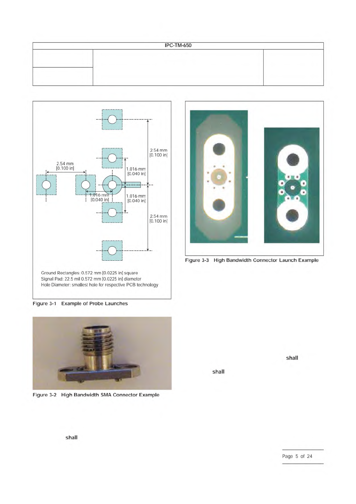
3.1.4 Probe Launch
The probe launch is comprised of a
PTH or other via structure and ground contact rectangular
pad and an example is depicted in Figure 3-1. The hole diam-
eter is recommended to be the smallest hole that is appropri-
ate for the respective technology. Some printed boards may
employ blind and buried vias. The recommended pitch
between ground and signal pad for high volume testing is
1.016 mm [0.040 in] or 2.54 mm [0.100 in]. Higher accuracy
can be achieved with smaller ground pad to signal pad spac-
ing and use of multiple ground vias.
3.1.5 Connector Launch
A high bandwidth connector
launch may be used instead of probe launch as show in Fig-
ure 3-2.
Figure 3-3 provides an example of high bandwidth connector
launch.
3.1.6 General Surface Condition
The panel test coupons
have the same surface plating and use the same solder
mask requirements as the functional printed board.
Number
2.5.5.12
Subject
Test Methods to Determine the Amount of Signal Loss on
Printed Boards
Date
07/12
Revision
A
IPC-TM-650
shall
shall
shall
Page
4
of
24
3.1.7 General Thieving
Thieving which is the use of
nonterminated copper structures, such as planes, pads,
and/or conductors adjacent to test lines that ensure plating
consistency may be used on test coupon. All thieving struc-
tures, if used,
be placed at least six times the width of
the signal conductor (of the test interconnect) or 2.5 mm
[0.100 in], whichever is greater, from each test interconnect.
3.1.8 Termination Types of Test Lines
There are two
types of line styles that may be used. The first is terminated on
each end with a launch. These lines are the only type that are
employed with the SPP and VNA method. The second type of
line is terminated on one end with a launch while the other end
is just the end of a conductor e.g., unterminated. The EBW
and RIE method may use either terminated or unterminated
lines types. The SET2DIL structure requires no termination.
3.1.9 Test Line Routing
The test lines be routed
over/under contiguous ground/voltage planes. The test line
conductors
be kept at least six times the height of the
laminate layer thickness which is closest to the conductor or
2.54 mm [0.100 in], whichever is greater; from printed board
structures include voids, plane splits, other conductors, and
holes.
It is recommended that test lines be straight.
3.1.10 Environmental Conditioning: Temperature and
Humidity
Temperature and humidity effect loss measure-
ments. Consistent results can be obtained by storing test
IPC-25512-3-1
IPC-25512-3-3
Number
2.5.5.12
Subject
Test Methods to Determine the Amount of Signal Loss on
Printed Boards
Date
07/12
Revision
A
IPC-TM-650
—
Ground
Rectangles:
0.572
mm
[0.0225
in]
square
Signal
Pad:
22.5
mil
0.572
mm
[0.0225
in]
diameter
Hole
Diameter:
smallest
hole
for
respective
PCB
technology
Figure
3-1
Example
of
Probe
Launches
Figure
3-2
High
Bandwidth
SMA
Connector
Example
Figure
3-3
High
Bandwidth
Connector
Launch
Example
shall
shall
Page
5
of
24