IPC-TM-650 EN 2022 试验方法--.pdf - 第436页
The layo ut of the disc structure is shown in Figure 3-4. The red text is on the external surf ace for pad identification pur- po ses. In a multi -signa l lay er cro ss secti on, disk s can be ‘‘ s ta c ke d’ ’ v er ti c…

specimens at 23 °C (± 2 °C) [73.4 °F (± 3.6 °F)] and 40% RH
(± 5% RH) for no less than 48 hours.
3.1.11 Fiberweave
It is recommended that the test con-
ductors route at an angle 10 degrees to glass cloth weave.
3.2 Probing
If probing is performed manually, operators
are urged to monitor the oscilloscope trace to ensure proper
connectivity. In the case of SMA connectors that are slip-fit, it
must be ensured that the amplitude of the detected pulse is
unchanged even when a small additional force is applied to
the holding stage movement (within the tolerance of the set-
up) for accurate, repeatable results. In the case of coaxial
probes, a small increase of the z-micropositioner travel (within
the tolerance of the probe allowed force) should also not
change the shape of the pulse. Automated probing can
improve the contact reliability.
For the most part the FD measurements do not use TDR
probes. They employ either connector or microprobes that
have respective calibration kits.
3.3 Test Coupon Characteristics
3.3.1 Test Line Impedance
It is recommended to use
lines that are 50 Ω single ended or 100 Ω differential for SPP.
Using other impedance lines are permitted but the applicabil-
ity is the responsibility or the user. EBW, RIE, SET2DIL, and
FD methods can use other impedances. It is recommended to
limit the line characteristic impedance Z
0
nonuniformity as
measured in TDR to not exceed 20% peak-to-peak along the
length of the lines. The difference in impedance between the
two lines used for SPP and RIE measurement
exceed 5%.
3.3.2 EBW Test Lines
Test lines for EBW be greater
than 5.08 cm [2.00 in] in length. Longer test interconnects
occupy more printed board or panel area. For short intercon-
nects, the relative impact of via loss to other loss effects may
be disproportionably large.
3.3.3 RIE Test Lines
The RIE test sample contain
one transmission (or interconnect) test structure and one ref-
erence transmission line per layer. The Reference is recom-
mended to be 2.54 cm [1.00 in]. The test line
be
between 15.24 cm [6.00 in] and 30.49 cm [12.0 in]. The spe-
cific length
be specified by printed board customers or
vendors. If fold back is required for striplines because of lim-
ited printed board area, maintain maximum spacing of 0.254
cm [0.10 in] between loop back trace legs. Foldbacks are not
recommended for microstrip structures.
3.3.4 SPP Test Structures
SPP test structures have
the following attributes:
• Conductors of varying lengths
• Signal – Ground launch/capture structures
• Disc structures to be used for low frequency capacitance
measurements
3.3.4.1 SPP Test Lines
The goal is to compare the cap-
tured waveforms from two conductors which are as identical
in cross section and laminate building blocks as the manufac-
turing process allows.
The SPP technique relies on the extraction of waveforms from
two different conductor lengths. The specific conductor
lengths used are dependent on the application.
The ratio of the lengths of the long and short conductors
at least be three to one. The following are recommended:
a) 3.0 cm [1.181 in] and 10.0 cm [3.937 in] conductor com-
bination. This combination provides the best output, but it
can be slightly more difficult to find conductors which are
well matched in their physical structure.
b) 2.0 cm [0.787 in] and 8.0 cm [3.149 in] conductor combi-
nation. This combination is useful in thin cards (<0.10 cm
[0.04 in]) for extended high-frequency range when using
coaxial probes for contact.
c) 5.0 cm [1.969 in] and 15.24 cm [6.00 in] conductor com-
bination. This combination is suited for production floor test
coupons.
Printed boards over 0.254 cm [0.1 in] thick
use micro-
vias, back-drilling, top milling or blind vias in order to reduce
the end discontinuities.
3.3.4.2 SSP Disc Structure
A 12.7 mm [0.5 in] diameter
disc is included in the signal layer artwork. The 1 MHz capaci-
tance of this disc is assessed using an LCR meter. The disc
capacitance is assessed through adjacent PTHs, one of which
is attached to the disc by a short conductor; the other is
attached to the reference planes. In the event that both planes
are not at the same reference potential, an isolation border is
placed around the disc structure to prevent shorting two dif-
ferent reference levels.
A ‘‘dummy’’ PTH/conductor structure which is of the same
design as the PTH/conductor used to access the disk is also
included. The capacitance of this dummy structure is sub-
tracted from the capacitance of the disc structure.
Number
2.5.5.12
Subject
Test Methods to Determine the Amount of Signal Loss on
Printed Boards
Date
07/12
Revision
A
IPC-TM-650
shall
not
shall
shall
shall
shall
shall
Page
6
of
24
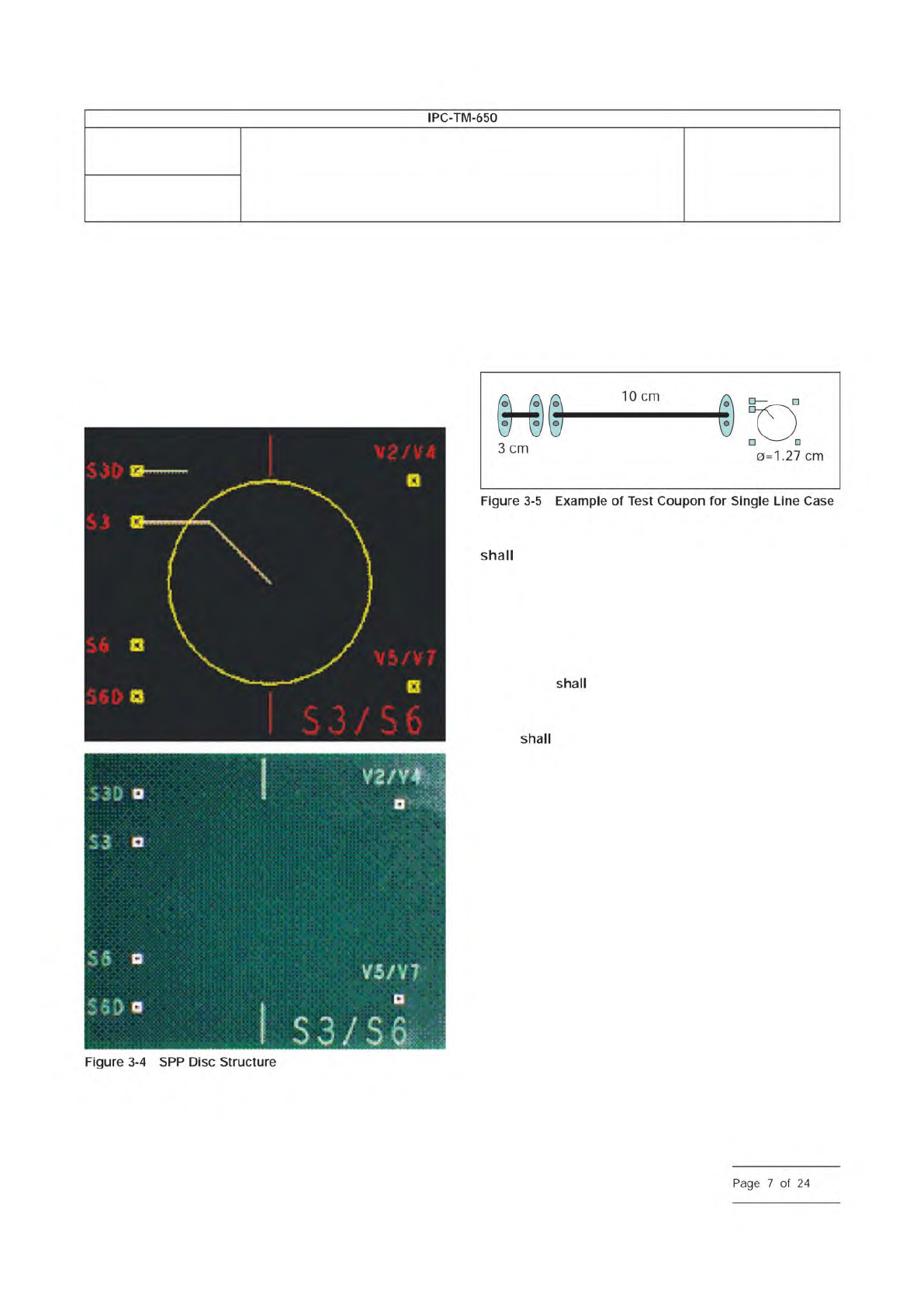
The layout of the disc structure is shown in Figure 3-4. The
red text is on the external surface for pad identification pur-
poses. In a multi-signal layer cross section, disks can be
‘‘stacked’’ vertically to facilitate later cross-sectioning if
desired (e.g., the disc for layer 6 is directly under the disc for
layer 3). The voltage planes around each disc are connected
together at the reference PTH and isolated from the rest of the
test vehicle through the use of a voltage divider.
3.3.4.3 SPP Test Coupon Design
An example is shown of
a typical coupon layout with 3 cm and 10 cm [1.18 in and
3.94 in] long lines and the 12.7 mm [0.5 in] disc in Figure 3-5.
The contacts are shown using the SMA connectors described
in Figure 3-3. This is a minimum configuration. Additional lines
would need to be added for differential line testing. The layout
in Figure 3-5 requires 2.0 cm x 16 cm [0.8 in x 6.3 in] of card
space.
3.3.5 SET2DIL Test Lines
The SET2DIL test coupons
contain one DUT (Device Under Test) for each
impedance/layer combination being controlled, and a ‘‘thru’’
reference structure.
3.3.6 FD Test Lines
The FD test sample shall contain one
transmission (or interconnect) test line per layer. The reference
line shall be between 1.27 cm [0.5 in] and 2.54 cm [1 in].
The test line
be between 15.24 cm [6 in] and 30.49 cm
[12 in]. The recommended line is 1.27 cm [0.5 in] for the ref-
erence line and 20.32 cm [8 in] for the test line. The specific
length be specified by printed board customers or ven-
dors.
3.3.7 Surface Finish
No matter what surface finish is
used, one should ensure the surface of the launch/capture
structure is clean and that the contact of the probes is not
affected by residues and/or oxides. OSP (organic solderability
preservative) finishes may inhibit probing of fine-pitched
probes and may need to be removed from the probe area.
In the lab based qualification/verification assessment, one can
facilitate this by slight burnishing (a pencil eraser often works
well), followed by cleaning with isopropyl alcohol (IPA).
In production floor assessments, the probe design should be
designed to break through any potential oxides or contami-
nants.
4 Apparatus
4.1 Differential and Single Ended Measurements
Both
single ended and differential measurement can be applied to
all the test methods. The measurement process for a differen-
tial measurement is identical to that of a single ended test. For
IPC-25512-3-5
Number
2.5.5.12
Subject
Test Methods to Determine the Amount of Signal Loss on
Printed Boards
Date
07/12
Revision
A
IPC-TM-650
Figure
3-4
SPP
Disc
Structure
shall
shall
shall
Page
7
of
24
the RIE, SPP, and EBW methods the differential voltage mea-
surement is used where the single ended measurement is
specified. For SET2DIL, a slightly different algorithm is used
for single-ended (S21) vs. differential (SDD21) signals. For the
FD (VNA) method, SDD21 is used in place of S21.
4.1.1 TDR Differential Channel Synchronization
The
two excitation channels need to be synchronized and have
the same amplitude. One recommended method is to use an
oscilloscope that has timing adjustments both in the TDR
heads and in the detector heads. Such a setup is performed
on a short pair of lines or zero-delay configuration. The steps
are as follows:
1) Channel 1 on the source side is propagated and detected
by Channel 3 on the detect side. The pulse or step is
recorded and displayed on the screen. Next, Channel 2 on
the source side is propagated to Channel 3 on the detect
side. The new pulse or step is overlapped with the one on
the screen. If there is a difference, the differential TDR skew
is adjusted until they are coincident. This makes sure that
the two sources do not have any difference in time, as
illustrated in Figure 4-1.
2) Next, the detector channels are adjusted. Channel 1 on the
source side is propagated and detected at this time by
Channel 4 on the detect side. This is compared to the
pulse or step obtained by the path of 1 going into 3. If they
are not synchronized, the Horizontal Skew Adjustment is
used to bring the timings together. Similarly, Channel 3 (or
4) is used as a source into channels 1 & 2; channel 2’s
horizontal skew is adjusted to bring the timings together,
see Figure 4-2. If there is any amplitude difference due to
detector amplification difference, the Channel 4 (or 2)
attenuation can be adjusted to match the waveform of
Channel 3 (or 1).
Both setup steps are needed for TDT and SPP; the first step
alone is enough for TDR used in RIE and EBW; and only step
2 is required for SET2DIL. Step 1 is repeated for Odd-Mode
and for Even-Mode measurements in the differential case.
Channel 2’s excitation must be in the same mode that
will be used during measurements (even or odd) during syn-
chronization; the pulse timing may vary, depending on the
excitation mode. Using a math function to invert the waveform
at the receiver might be necessary for odd mode excitation.
IPC-25512-4-1
1
2
3
IPC-25512-4-2
1
3
4
3
1
2
Number
2.5.5.12
Subject
Test Methods to Determine the Amount of Signal Loss on
Printed Boards
Date
07/12
Revision
A
IPC-TM-650
Note:
Page
8
of
24