IPC-TM-650 EN 2022 试验方法--.pdf - 第463页
Figure 6 Clamp Arrangement (See 5.1.5) Showing Side a nd Front Views for Specimen Lengths of 76.2 mm and 304.8 mm Figure 7 Copper Fitting with R everse Bevel (S ee 5.2.2) Soldered to the 1.8 mm Semi-Rigid Co axial Cable …
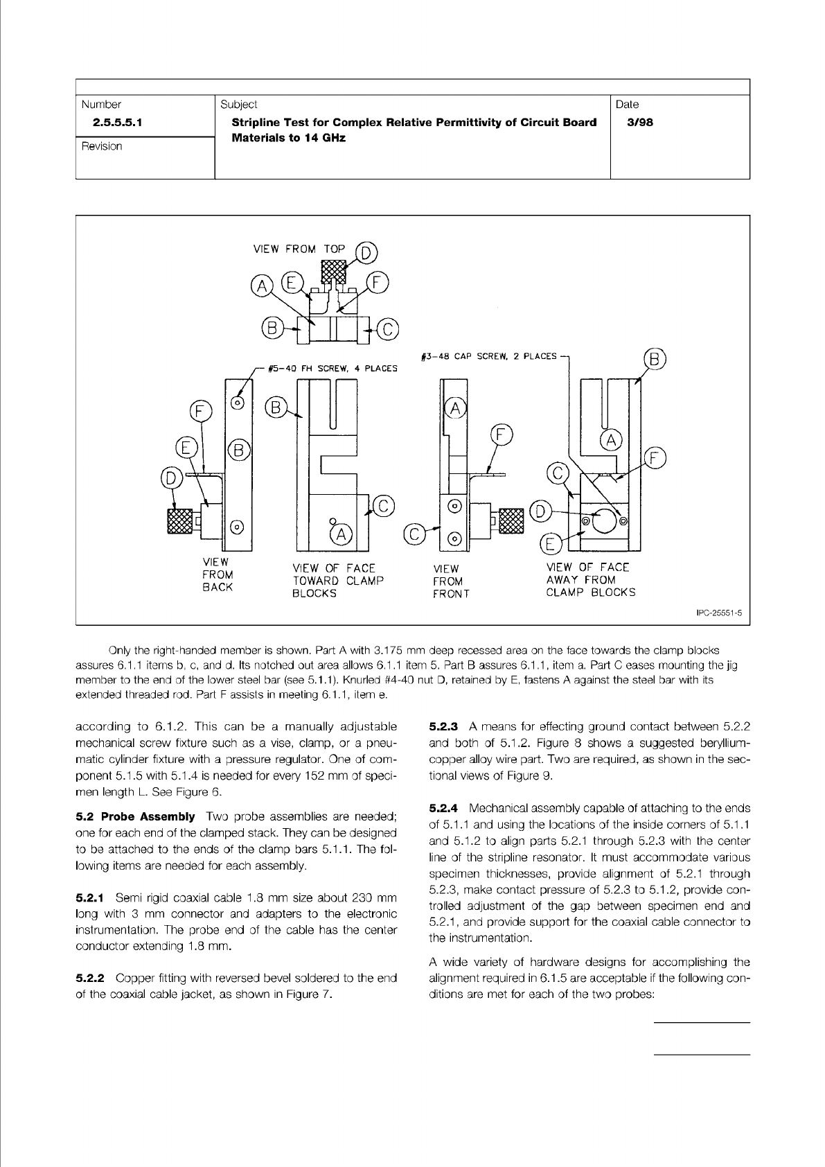
Figure 5 Five Assembly Views for a Suggested Two Member Stacking Alignment Jig (See 5.1.3)
Note:
IPC-TM-650
Page 5 of 11
Number
2.5.5.5.1
Revision
Subject
Stripline
Test
for
Complex
Relative
Permittivity
of
Circuit
Board
Materials
to
14
GHz
Date
3/98
VIEW
FROM
BACK
VIEW
OF
FACE
TOWARD
CLAMP
BLOCKS
厂
#5-40
FH
SCREW,
4
PLACES
FRONT
CLAMP
BLOCKS
IPC-25551-5
Only
the
right-handed
member
is
shown.
Part
A
with
3.175
mm
deep
recessed
area
on
the
face
towards
the
clamp
blocks
assures
6.1
.1
items
b,
c,
and
d.
Its
notched
out
area
allows
6.1
.1
item
5.
Part
B
assures
6.1
.1
,
item
a.
Part
C
eases
mounting
the
jig
member
to
the
end
of
the
lower
steel
bar
(see
5.1
.1).
Knurled
#4-40
nut
D,
retained
by
E,
fastens
A
against
the
steel
bar
with
its
extended
threaded
rod.
Part
F
assists
in
meeting
6.1
.1
,
item
e.
according
to
6.1.2.
This
can
be
a
manually
adjustable
mechanical
screw
fixture
such
as
a
vise,
clamp,
or
a
pneu¬
matic
cylinder
fixture
with
a
pressure
regulator.
One
of
com¬
ponent
5.1
.5
with
5.1
.4
is
needed
for
every
152
mm
of
speci¬
men
length
L.
See
Figure
6.
5.2
Probe
Assembly
Two
probe
assemblies
are
needed;
one
for
each
end
of
the
clamped
stack.
They
can
be
designed
to
be
attached
to
the
ends
of
the
clamp
bars
5.1.1.
The
fol¬
lowing
items
are
needed
for
each
assembly.
5.2.1
Semi
rigid
coaxial
cable
1.8
mm
size
about
230
mm
long
with
3
mm
connector
and
adapters
to
the
electronic
instrumentation.
The
probe
end
of
the
cable
has
the
center
conductor
extending
1.8
mm.
5.2.2
Copper
fitting
with
reversed
bevel
soldered
to
the
end
of
the
coaxial
cable
jacket,
as
shown
in
Figure
7.
5.2.3
A
means
for
effecting
ground
contact
between
5.2.2
and
both
of
5.1
.2.
Figure
8
shows
a
suggested
beryllium¬
copper
alloy
wire
part.
Two
are
required,
as
shown
in
the
sec¬
tional
views
of
Figure
9.
5.2.4
Mechanical
assembly
capable
of
attaching
to
the
ends
of
5.1
.1
and
using
the
locations
of
the
inside
corners
of
5.1
.1
and
5.1.2
to
align
parts
5.2.1
through
5.2.3
with
the
center
line
of
the
stripline
resonator.
It
must
accommodate
various
specimen
thicknesses,
provide
alignment
of
5.2.1
through
5.2.3,
make
contact
pressure
of
5.2.3
to
5.1.2,
provide
con¬
trolled
adjustment
of
the
gap
between
specimen
end
and
5.2.1
,
and
provide
support
for
the
coaxial
cable
connector
to
the
instrumentation.
A
wide
variety
of
hardware
designs
for
accomplishing
the
alignment
required
in
6.1.5
are
acceptable
if
the
following
con¬
ditions
are
met
for
each
of
the
two
probes:
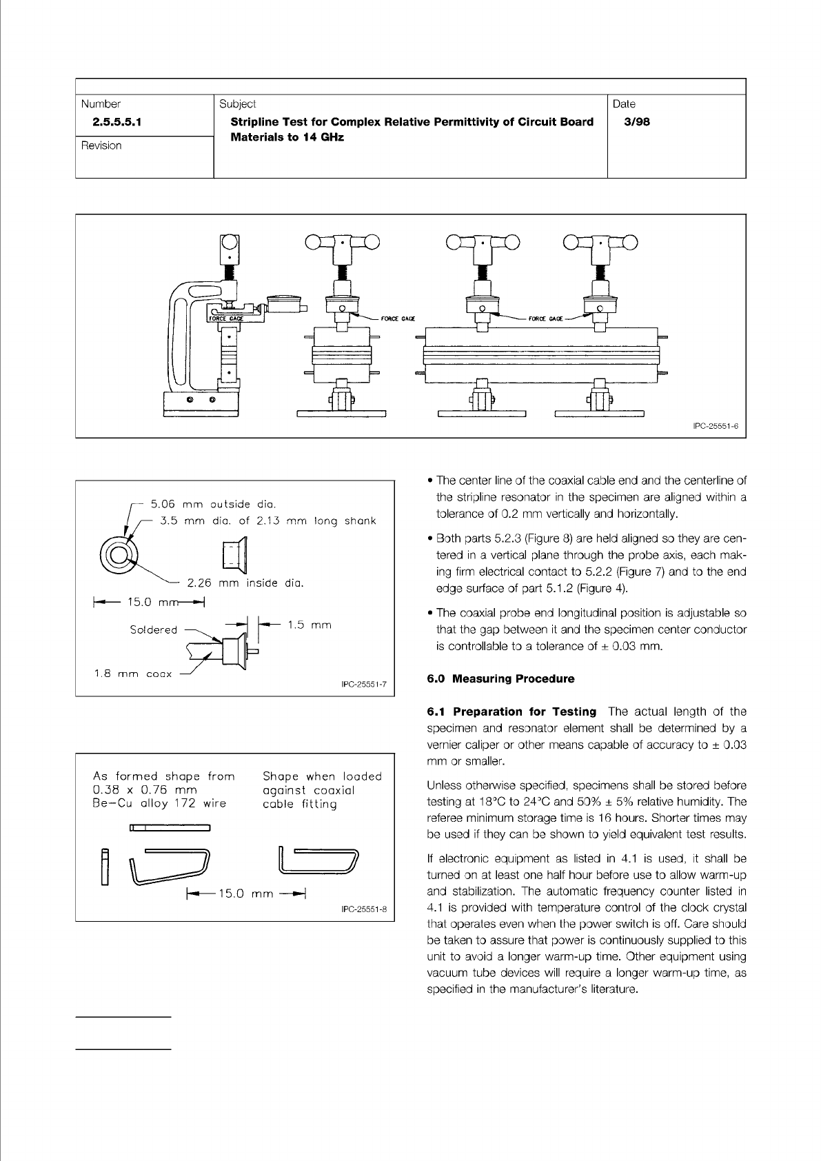
Figure 6 Clamp Arrangement (See 5.1.5) Showing Side and Front Views for Specimen Lengths of 76.2 mm and 304.8 mm
Figure 7 Copper Fitting with Reverse Bevel (See 5.2.2)
Soldered to the 1.8 mm Semi-Rigid Coaxial Cable Probe
Figure 8 Formed Be-Cu Alloy Wire for Ground Continuity
from Coaxial Cable Fitting to Copper Ground Plate
IPC-TM-650
Page 6 of 11
Number
2.5.5.5.1
Revision
Subject
Stripline
Test
for
Complex
Relative
Permittivity
of
Circuit
Board
Materials
to
14
GHz
Date
3/98
IPC-25551-6
As
formed
shape
from
0.33
x
0.76
mm
Be—
Cu
alloy
1
72
wire
Shape
when
loaded
against
coaxial
cable
fitting
H
—
1
5.0
mm
—
H
IPC-25551-8
•
The
center
line
of
the
coaxial
cable
end
and
the
centerline
of
the
stripline
resonator
in
the
specimen
are
aligned
within
a
tolerance
of
0.2
mm
vertically
and
horizontally.
•
Both
parts
5.2.3
(Figure
8)
are
held
aligned
so
they
are
cen¬
tered
in
a
vertical
plane
through
the
probe
axis,
each
mak¬
ing
firm
electrical
contact
to
5.2.2
(Figure
7)
and
to
the
end
edge
surface
of
part
5.1.2
(Figure
4).
•
The
coaxial
probe
end
longitudinal
position
is
adjustable
so
that
the
gap
between
it
and
the
specimen
center
conductor
is
controllable
to
a
tolerance
of
土
0.03
mm.
6.0
Measuring
Procedure
6.1
Preparation
for
Testing
The
actual
length
of
the
specimen
and
resonator
element
shall
be
determined
by
a
vernier
caliper
or
other
means
capable
of
accuracy
to
土
0.03
mm
or
smaller.
Unless
otherwise
specified,
specimens
shall
be
stored
before
testing
at
18℃
to
24℃
and
50%
±
5%
relative
humidity.
The
referee
minimum
storage
time
is
16
hours.
Shorter
times
may
be
used
if
they
can
be
shown
to
yield
equivalent
test
results.
If
electronic
equipment
as
listed
in
4.1
is
used,
it
shall
be
turned
on
at
least
one
half
hour
before
use
to
allow
warm-up
and
stabilization.
The
automatic
frequency
counter
listed
in
4.1
is
provided
with
temperature
control
of
the
clock
crystal
that
operates
even
when
the
power
switch
is
off.
Care
should
be
taken
to
assure
that
power
is
continuously
supplied
to
this
unit
to
avoid
a
longer
warm-up
time.
Other
equipment
using
vacuum
tube
devices
will
require
a
longer
warm-up
time,
as
specified
in
the
manufacturer's
literature.
available based on equation (1). Note that the de-embedded
insertion loss is defined with a reference impedance of the
transmission line.
1.3 General Calibration/de-embedding Methods to Set
up Correct Reference Plane for Printed Board Conduc-
tor Insertion Loss Characterization
As mentioned earlier,
there are existing calibration/de-embedding methods for gen-
eral purpose interconnect characterization to move the cali-
bration reference plane to printed board interfaces. These
methods are validated by the industry, and therefore included
herein, although they are either more complicated or costly
than the Eigen-value based method.
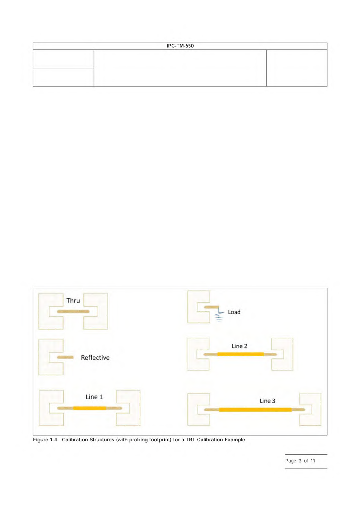
1.3.1 TRL Calibration
The TRL (and its variants such as
LRM) method [7] is a general approach to move the calibra-
tion reference plane from the coaxial connector to printed
board interfaces. Figure 1-4 shows the typical calibration
structures for a TRL calibration, with microwave probe foot-
print (with single-ended probing as an example). The TRL cali-
bration technique only relies on the characteristic impedance
of the transmission line and does NOT need the parasitics of
Reflective Standard to be known, nor propagation delay of
Line. A typical TRL calibration structure may also include a
Load structure that works only at very low frequencies, and
additional Line structures to cover a wide frequency range.
Most VNAs offer TRL calibration options, please refer to the
manual or application note for your specific equipment to per-
form a TRL calibration.
TRL calibration has been widely used in the industry since the
technique no longer requires accurate calibration termination
standards. This overcomes the difficulties of SOLT calibration,
and the reference plane can be moved to the printed board.
However, there are still some disadvantages to the TRL cali-
bration. For example, there are many components of the cali-
bration standard to handle. This takes substantial printed
board area and requires tedious calibration process in the lab,
while being prone to the operator error. Additionally, the TRL
technique requires accurate characteristic impedance specifi-
cation for the line standard, which is problematic to determine
in a dispersive environment.
1.3.2 2X-Thru De-embedding
In the last decade, the
2X-thru de-embedding methodology is gaining popularity due
to its simplicity of test fixture design and de-embedding pro-
cedures [8]. In contrast to the TRL calibration technique,
which requires measurement of multiple structures as shown
in Figure 1-4, 2X-Thru De-embedding requires only one
de-embedding structure.
The basic idea of the 2X-Thru de-embedding approach is
shown in Figure 1-5. The S-parameters of the 2X-thru
IPC-25514-1-4
Number
2.5.5.14
Subject
Measuring High Frequency Signal Loss and Propagation on
Printed Boards with Frequency Domain Methods
Date
02/2021
Revision
IPC-TM-650
—
Thru
Reflective
Line
1
Figure
1-4
Calibration
Structures
(with
probing
footprint)
for
a
TRL
Calibration
Example
Page
3
of
11