IPC-TM-650 EN 2022 试验方法--.pdf - 第490页
1 Sc op e T he d i el ec tr ic s tr e ng th t es t ( al so c a ll ed hi gh - potential [Hi-Pot], over potential, or voltage breakdown) con- sists of the ap plication of a test voltage for a sp ecific time between mut ual…
IPC-TM-650
Number
Subject Date
Revision
Page 3 of 3
2.5.6
Dielectric
Breakdown
of
Rigid
Printed
Wiring
Material
5/86
B
6.1
The
dielectric
breakdown
of
the
material
may
be
adversely
affected
if
the
drilling
process
used
to
produce
the
holes
is
inadequate.
Use
of
a
sharp
high
speed
drill
is
recom¬
mended
to
prevent
burning
the
material
or
producing
rough
holes.
6.2
This
test
requires
voltages
which
are
life
threatening.
The
High
Voltage
Tester
must
be
installed
and
operated
in
accor¬
dance
with
the
manufacturer's
instructions.
If
the
test
cham¬
ber
is
not
totally
enclosed,
with
a
safety
interlock,
extreme
care
must
be
exercised
in
performance
of
the
test.
1 Scope
The dielectric strength test (also called high-
potential [Hi-Pot], over potential, or voltage breakdown) con-
sists of the application of a test voltage for a specific time
between mutually insulated portions of a printed board or
between insulated portions and ground. This is used to prove
that the printed board can operate safely at its rated voltage
and withstand momentary overpotentials due to switching,
surges, and other similar phenomena.
2 Applicable Documents
Standard Test Method for Dielectric Break-
down Voltage and Dielectric Strength of Solid Electrical Insu-
lation Materials at Commercial Power Frequencies
3 Test Specimen
Three 102 mm x 102 mm [4.016 in x
4.016 in] squares of glass epoxy laminate materials having
1 ounce (0.0343 mm [0.00135 in] nominal) copper foil lami-
nates on one side, and having the test specimen polymer film
applied to the copper surface (see specimen preparation).
4 Apparatus
4.1
Any high voltage potential test equipment capable of
providing voltage increases of 500 VDC per second, up to at
least 10,000 VDC (see Section 6).
4.2
A standard Type 1 electrode per ASTM D 149, with a 51
mm [2.0 in] diameter, 25 mm [1.0 in] thick, with edges
rounded to 6.4 mm [0.25 in.] radius to cover the test surface.
5 Procedure
5.1 Preparation of Test Specimen
5.1.1
Cut the laminate specimen to 102 mm x 102 mm
[4.016 in x 4.016 in] and sand the edges lightly.
5.1.2
If double clad material is used, etch off all copper foil
on one side.
5.1.3
Clean the copper foil surface thoroughly, per the poly-
mer manufacturer’s recommendations, prior to applying poly-
mer coating.
5.1.4
Apply a film of the polymer test material on an area of
76.2 mm x 76.2 mm [3.0 in x 3.0 in] at the center of the cop-
per clad surface. A pinhole free film is essential.
5.1.5
Cure the polymer coating per manufacturer’s recom-
mendations.
5.2 Test
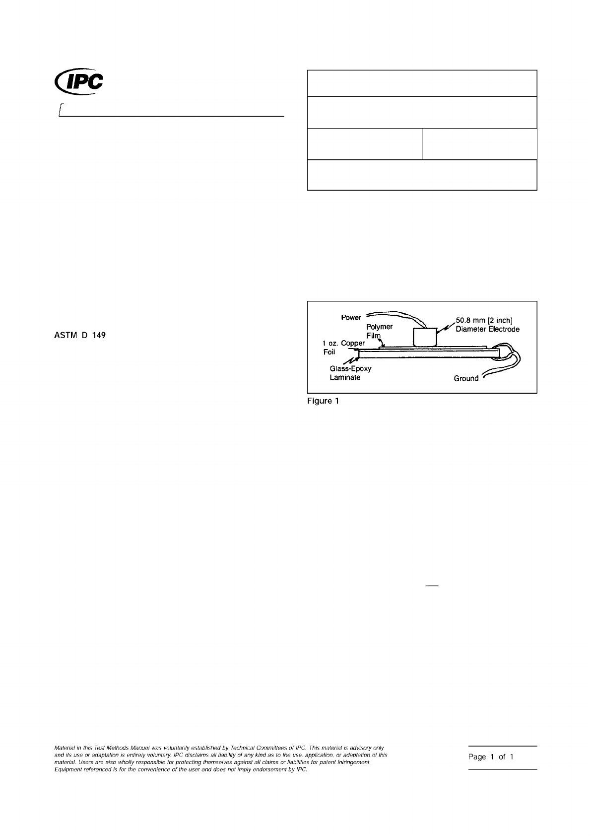
5.2.1
Clip the ground terminal of the tester over the thick-
ness of the copper foil and substrate, being careful not to let
the clip extend inward to the polymer coating (see Figure 1).
5.2.2
Place the positive electrode on top of test panel at the
center. Make certain the electrode and clip are electrically iso-
lated by the test polymer film.
5.2.3
Set up the potential voltage tester. Increase the volt-
age 500 VDC per second, until specimen exceeds require-
ment or breakdown occurs.
5.2.4
Measure the coating thickness of each of the test
specimens to the nearest 0.0025 mm [0.0001 in] in at least
four locations. Compute the average coating thickness and
standard deviation.
5.3 Evaluation
Determine the dielectric strength, E
D
, using:
E
D
=
V
BD
t
where t is the thickness of the specimen, to the nearest
0.0025 mm [0.0001 in], measured in 5.2.4 and V
BD
is
the breakdown voltage measured in 5.2.3. Record results as
‘‘V/mm’’ or ‘‘V/in.’’
6 Notes
6.1
Suggested source for tester: Hipotronics Model HD-140
from Hipotronics, Inc. Brewster, NY 10509, or equivalent.
6.2
Safety must be exercised because of the potential dan-
ger of electrical shock.
IPC-2561-1
3000 Lakeside Drive, Suite 309S
Bannockburn, IL 60015-1249
IPC-TM-650
TEST METHODS MANUAL
Number
2.5.6.1
Subject
Solder Mask - Dielectric Strength
Date
03/07
Revision
B
Originating Task Group
Solder Mask Performance Task Group (5-33b)
ASSOCIATION CONNECTING
ELECTRONICS INDUSTRIES
®
ASTM
D
149
Figure
1
Material
M
this
历
sf
Methods
Manual
was
voluntarily
established
by
Technical
Committees
of
IPC.
This
material
is
advisory
only
and
its
use
。厂
adaptation
is
entirely
voluntary.
IPC
disclaims
liability
of
any
k/nd
as
to
the
use,
application,
or
adaptation
of
this
material.
Users
are
also
wholly
responsible
for
protecting
themselves
against
claims
or
liabililies
for
patent
infringement.
Equipment
referenced
/s
for
the
convenience
of
the
user
and
does
not
imply
endorsement
by
IPC.
Page
1
of
1
IPC-TM-650
Page 23 of 23
Number
2.5.5.7
Subject
Characteristic
Impedance
of
Lines
on
Printed
Boards
by
TDR
Date
03/04
Revision
A
6.3.6.2
Probes
for
Coupled-Signal-Line
(Differential)
Transmission
Line
Measurements
The
probe
consider¬
ations
described
in
4.3.3
apply
for
probes
used
in
differential
transmission
line
measurements.
However,
the
necessity
to
simultaneously
probe
two
signal
lines
and
one
or
two
refer¬
ence
plane
contacts
makes
differential
probing
more
difficult
than
probing
single
signal
line
structures.
In
a
PCB
manufac¬
turing
environment,
the
use
of
two
probes
that
were
previ¬
ously
used
for
single-ended
measurements
may
not
be
pos¬
sible.
This
is
because
the
operator
is
required
to
use
both
hands
for
probing,
which
leaves
them
unable
to
operate
the
instrument.
Contact
your
instrument
manufacturer
for
their
probing
solutions
and
advice.
Probes
from
one
manufacturer
can
also
be
used
with
another
manufacturer's
TDR
if
the
impedance
values
and
connectors
are
compatible.
6.4
Adjustable
Measurement
Parameters
6.4.1
Sampling
Interval
(Point
Spacing)
The
temporal
resolution
of
the
TDR
unit
is
an
issue
only
if
it
impacts
the
duration
of
the
constant-
valued
regions
in
the
TDR
waveform
(see
4.1.2)
that
are
used
for
computing
Zo.
The
temporal
reso¬
lution
of
the
TDR
is
affected
by
the
transition
duration
of
the
TDR
step
response,
the
transition
duration
of
the
step
response
of
all
intervening
electrical
components
(connectors,
cables,
adapters),
measurement
jitter,
the
interval
between
sampling
instances,
and
timebase
errors.
For
typical
TDR
measurements,
timebase
errors
and
sampling
intervals
should
not
be
an
issue
(both
are
or
can
be
made
to
be
less
than
1
0
ps).
The
effect
of
measurement
jitter
can
be
modeled
by
con¬
volving
the
jitter
distribution
with
the
TDR
step
response
to
yield
an
effective
TDR
step
response.
The
effect
of
jitter
on
the
bandwidth
of
the
TDR
measurement
can
be
assessed
from
the
jitter
spectrum,
which
can
be
described
by:
j(/)
=
e-2(gf)2
where:
J
is
the
jitter
spectrum,
f
is
frequency,
and
a
is
the
rms
jitter
value
If
the
effective
step
response
impacts
the
duration
of
the
mea¬
surement
zones,
then
jitter
must
be
reduced.
If
the
jitter
has
an
observable
effect,
then
the
user
must
reduce
the
duration
of
the
measurement
zone
(by
increasing
the
lower
limit
and
decreasing
the
upper
limit,
(see
5.1.3)
from
which
Zo
is
com¬
puted
or
reduce
the
system
jitter.
Reduction
in
the
duration
of
the
measurement
zone
may
introduce
a
bias
in
the
voltage
or
reflection
coefficient
values
and
this
affect
the
computed
value
of
Zo.
If
the
rms
jitter
value
is
less
than
20
%
of
the
transition
duration
of
the
TDR
step
response,
then
the
jitter
is
small
and
can
be
ignored.
For
typical
TDR
systems,
however,
rms
jitter
is
less
than
10
ps
and
will
not
affect
the
Zo
measurements.
Similarly,
the
effect
of
cables,
connectors,
and
adapters
on
the
measurement
can
be
modeled
by
convolving
their
step
responses
with
that
of
the
TDR
unit.
If
the
transition
duration
of
this
new
step
response
meets
the
requirements
of
4.1.2,
then
the
performance
of
the
cables,
connectors,
and
adapters
is
adequate.
6.4.2
Waveform
Averaging
and
Number
of
Samples
in
the
Measurement
Zone
Waveform
averaging
reduces
the
effective
noise
level
of
the
measurement
by
M^72,
where
M
is
the
number
of
acquired
waveforms
(typically,
8
M
256).
Consequently,
averaging
can
reduce
measurement
noise.
This
reduction
is
limited
by
the
number
of
bits
of
the
analog-
to-digital
converter
of
the
TDR
system.
However,
if
the
TDR-
system
exhibits
drift
in
the
timebase,
averaging
too
many
waveforms
may
result
in
a
reduction
of
tsys
and
a
commensu¬
rate
reduction
in
the
temporal/spatial
resolution
of
the
TDR.
The
number
of
samples
(data
points)
in
the
measurement
zone
will
affect
the
standard
deviation
of
the
computed
value
of
Zo
because
this
value
is
the
result
of
averaging
all
the
samples
in
the
measurement
zone.
Therefore,
the
more
samples
in
the
measurement
zone,
the
smaller
will
be
the
standard
deviation
of
the
computed
Zo
value.
6.4.3
Selection
of
Constant-Valued
Region
(Measure¬
ment
Zone)
Inconsistency
in
defining
where
the
constant¬
valued
region
is
located
in
the
TDR
waveform
may
cause
a
significant
but
unknown
error
than
can
exceed
5.0
Q.
Speci¬
fying
the
measurement
zone
improves
measurement
repeat¬
ability
of
the
same
or
similar
samples,
and
this
can
improve
assessment
of
design
and
fabrication
quality
and
vendor
capability.
This
measurement
zone
should
be
far
enough
away
from
the
launch
and
the
open
end
of
the
transmission
line
under
test
to
minimize
the
effects
of
these
discontinuities.
The
measurement
zone
is
to
be
given
as
the
separation
between
two
positions
on
the
transmission
line,
and
these
positions
are
to
be
given
as
a
percentage
of
the
transmission
line
length
referenced
from
the
TDR/transmission
line
inter¬
face.
The
measurement
zone
is
defined
in
5.1
.3.
6.5
Acknowledgments
The
majority
of
the
figures
used
herein
were
provided
by
Mr.
Bryan
C.
Parker
of
the
Introbot-
ics
Corporation,
Albuquerque,
NM.