IPC-TM-650 EN 2022 试验方法--.pdf - 第504页
1 Scope The d ielec tri c withstanding voltage test (Hipot te st) consists of th e application of a voltage high e r than the oper- ating voltage for a specific time across the thickness of the test spe cim e n’s dielect…
IPC-TM-650
Page 2 of 2
Number
2.5.7.1
Subject
Dielectric
Withstanding
Voltage
-
Polymeric
Conformal
Coating
Date
07/00
Revision
5.1.2
Immerse
and
agitate
the
test
specimens
in
2-propanol
for
30
seconds.
Scrub
with
a
soft
bristle
brush
and
spray
with
clean
2-propanol.
5.1.3
Place
the
cleaned
specimens
in
an
oven
maintained
at
50℃
[1
22°F]
for
three
to
five
hours
to
dry.
5.1.4
Remove
the
specimens
from
the
oven
and
place
in
a
desiccator
to
cool.
5.1.5
Conformal
coat
the
test
specimens
and
cure
in
accor¬
dance
with
the
suppliers
recommendations.
If
the
specimens
are
not
used
immediately,
seal
the
specimens
in
Kapac®
bags.
5.2
Procedure
5.2.1
For
each
individual
specimen,
secure
all
the
positive
leads
(1
,
3
and
5)
together
and
the
negative
(2
and
4)
together.
5.2.2
Attach
the
leads
of
the
Hi-Pot
Tester
to
the
wires
of
the
test
specimen.
5.2.3
Raise
the
test
voltage
from
zero
to
1,500
VAC
at
1
00
VAC
per
second.
5.2.4
Apply
the
test
voltage
of
1
,500
VAC
at
50-60
Hz
for
one
minute
and
record
any
leakage
rate.
5.2.5
After
the
one-minute
duration,
turn
off
the
voltage
and
disconnect
the
test
specimen
from
the
Hi-Pot
Tester.
6.0
Evaluate
6.1
Record
if
the
specimen
exhibits
flashover,
sparkover
or
breakdown.
6.1.1
Record
the
leakage
current
of
each
specimen.
1 Scope
The dielectric withstanding voltage test (Hipot test)
consists of the application of a voltage higher than the oper-
ating voltage for a specific time across the thickness of the
test specimen’s dielectric layer. This is used to prove that a
printed board can operate safely at its rated voltage and with-
stand momentary voltage spikes due to switching, surges,
and other similar phenomena. Although this test is similar to a
voltage breakdown test, it is not intended for this test to cause
insulation breakdown. Rather, it serves to determine whether
the test specimen’s layers have adequate withstanding volt-
age. This document is applicable to thin dielectric materials
such as those defined by IPC-4821.
The results can be indicative of a change or a deviation from
the normal material characteristics resulting from manufactur-
ing, processing or aging conditions. The test is useful for qual-
ity acceptance and in the determination of the suitability of the
material for a given application and may be adapted for pro-
cess control.
2 Applicable Documents
Specification for Embedded Passive Device
Capacitor Materials for Rigid and Multilayer Printed Boards
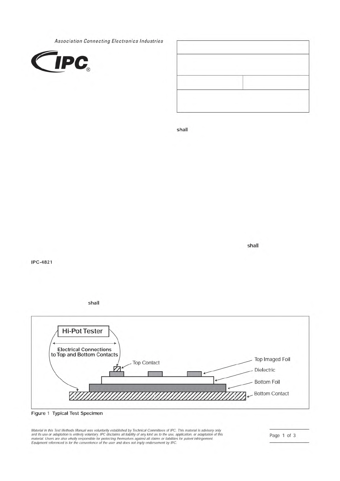
3 Test Specimen
3.1 Qualification Testing
For laminate-like capacitor
materials, test specimens
be 50 mm [1.97 in] diameter
circular electrodes (see ‘‘Top Imaged Foil’’ in Figure 1) that
be formed by imaging and then etching the copper foil,
unless otherwise as agreed upon by user and supplier
(AABUS). Spacing between adjacent Top Imaged Foil con-
ductors is recommended to be ≥100 times the dielectric thick-
ness. In order to avoid field gradient and mechanical stress
concentration, which can cause faulty dielectric breakdown,
the Bottom Foil can be either a circle larger than the Top
Imaged Foil or can be a continuous copper sheet. The con-
tinuous copper sheet will be required for very thin capacitor
dielectric layers that are not self-supporting.
For nonlaminate-like capacitor materials, the test specimen’s
Top Imaged Foil can be a size other than a 50 mm [1.97 in]
diameter circle, if this size is not practical or typical. The test
specimen’s Top Imaged Foil size for these nonlaminate-like
materials should be set to the largest size normally recom-
mended for this product (see 5.2.4). The thickness for the test
specimens should be the typical/recommended thickness. A
minimum of five test specimens
be tested for qualifica-
tion.
3.2 Conformance Testing
Test specimens can be the
same as used for qualification testing or can be other sizes or
shapes. For testing in printed board environments, actual
innerlayer power and ground features are typically used,
although other board features or test specimens can also be
used. Please note that adjustments for capacitor plate size are
required in the test procedure (see Section 6).
IPC-2572-1.eps
3000 Lakeside Drive, Suite 309S
Bannockburn, IL 60015-1249
IPC-TM-650
TEST METHODS MANUAL
Number
2.5.7.2
Subject
Dielectric Withstanding Voltage (Hipot Method) -
Thin Dielectric Layers for Printed Boards
Date
11/2009
Revision
A
Originating Task Group
Embedded Devices Test Methods Subcommittee
(D-54)
Association
Connecting
Electronics
Industries
shall
IPC-4821
shall
shall
Top
Imaged
Foil
Dielectric
Bottom
Foil
Bottom
Contact
Figure
1
Typical
Test
Specimen
Material
/n
this
Test
Methods
Manual
was
voluntarily
established
by
Technical
Committees
of
I
PC.
This
material
/s
advisory
only
and
"s
use
or
adaptation
,
s
entirely
voluntary.
IPC
disclaims
all
liability
of
any
kind
as
to
the
use,
application,
or
adaptation
of
this
material.
Users
are
also
wholly
responsible
for
protecting
themselves
against
all
claims
or
liabilities
for
patent
infringement.
Equipment
referenced
/s
for
the
convenience
of
the
user
and
does
not
imply
endorsement
by
IPC.
Page
1
of
3
1 Scope
This method specifies time domain reflectometry
(TDR) methods for measuring and calculating the propagation
delay of uniform, controlled impedance transmission lines fab-
ricated in printed board (PB) technology. The method defines
a propagation delay per unit length t
D
by specifying how to
measure the time it takes a signal to propagate a given length
of transmission line.
This method describes methods that utilize TDR measure-
ments of multiple, unterminated test lines that are designed to
differ only in length. A TDR signal, usually a step waveform
1
,
is injected into a transmission line or lines and the reflection
response is measured some time later. This method shows
how t
D
is determined as the difference between the time it
takes a TDR pulse to reflect from the unterminated ends of
two transmission lines divided by the length difference of the
two lines.
1.1 Applicability
Engineering development of high-speed
and high-frequency electronic circuits and systems requires
detailed information on the electrical performance of PBs to
assure that transmission line designs yield the expected per-
formance characteristics. Detailed analysis of the design and
fabrication variations expected throughout manufacturing
assures that a proposed design can be manufactured at a
useful quality level. Measuring and characterizing propagation
delay on transmission line test structures is a direct means of
assessing the success of the PB transmission line model.
Since transmission line measurements are affected by imped-
ance conditions at the transmission line boundaries, propaga-
tion measurements specified here may not return the actual
delay observed for a given application. The procedures test
whether uniform, impedance controlled PB transmission lines
exhibit the expected propagation delay based on an electrical
model or reference test structures.
This method is generally applicable to uniform transmission
lines fabricated with commercial PB processes (see IPC-
2141), and is also useful for various transmission lines and
material systems studied at the research and development
stages.
The method is applicable when:
• Electrical contacts (connectors or probes) are readily made
to the transmission lines test structures
• Transmission line characteristic impedance is neither
extremely high nor low compared to the instrument’s test
port impedance
• Transmission line propagation loss sets acceptable signal-
to-noise ratios for the measured signals
The current version of this method specifies singled-ended
TDR measurements of unbalanced transmission lines, though
the method is sufficiently general to be extended to differential
TDR measurements of balanced lines.
1.2 Measurement System Limitations
Applying a speci-
fied test method helps assure accurate and consistent propa-
gation delay results, however measurements of propagation
delay can vary depending on equipment used. Known mea-
surement system limitations include:
a. Electrical noise of the TDR receiver, limiting propagation
delay accuracy and repeatability when signal levels are low
b. Trigger, source, and receiver jitter in the TDR instrument,
limiting temporal resolution
c. Drift in the trigger point of the TDR sources limiting, tempo-
ral resolution
d. Slow TDR pulse rise times, limiting temporal resolution
e. Waveform distortion induced by the low-quality test set-up
cables, connectors, and the signal launch points, inducing
errors in the reported propagation delay
Further measurement system considerations and notes are
provided in Section 6.
1.3 Sample Limitations
The type of test sample used may
also impact propagation delay accuracy. The sample-based
limitations include:
a. Lines on a fabricated PB deviating significantly from
design. For example, microstrip lines longer than 15.0 cm
[5.91 in] on PBs with plated-through holes (PTH) often
have variations in line width due to nonuniform plating
and/or etching. This makes the uniform transmission line
1. The signals used in the TDR system are actually rectangular pulses; because the measured duration of the TDR waveform is much less than the actual pulse
duration, the TDR waveform appears to be a step function.
3000 Lakeside Drive, Suite 309S
Bannockburn, IL 60015-1249
IPC-TM-650
TEST METHODS MANUAL
Number
2.5.5.11
Subject
Propagation Delay of Lines on Printed Boards by
TDR
Date
04/2009
Revision
Originating Task Group
Propagation Delay Test Methods Task Group
(D-24a)
ASSOCIATION CONNECTING
ELECTRONICS INDUSTRIES
®
Material
/n
this
Test
Methods
Manual
was
voluntarily
established
by
Technical
Committees
of
I
PC.
This
material
/s
advisory
only
and
"s
use
or
adaptation
,
s
entirely
voluntary.
IPC
disclaims
all
liability
of
any
kind
as
to
the
use,
application,
or
adaptation
of
this
material.
Users
are
also
wholly
responsible
for
protecting
themselves
against
all
claims
or
liabilities
for
patent
infringement.
Equipment
referenced
/s
for
the
convenience
of
the
user
and
does
not
imply
endorsement
by
IPC.
Page
1
of
16