IPC-TM-650 EN 2022 试验方法--.pdf - 第508页
interconnects, but a practical issue of o perator ability to use han d-he ld pr obe s may be co nsid ered . Tes t rep orts m ust report any de viation from the nominal contact land and PTH geometry. 3.9 Contact Land Pitc…
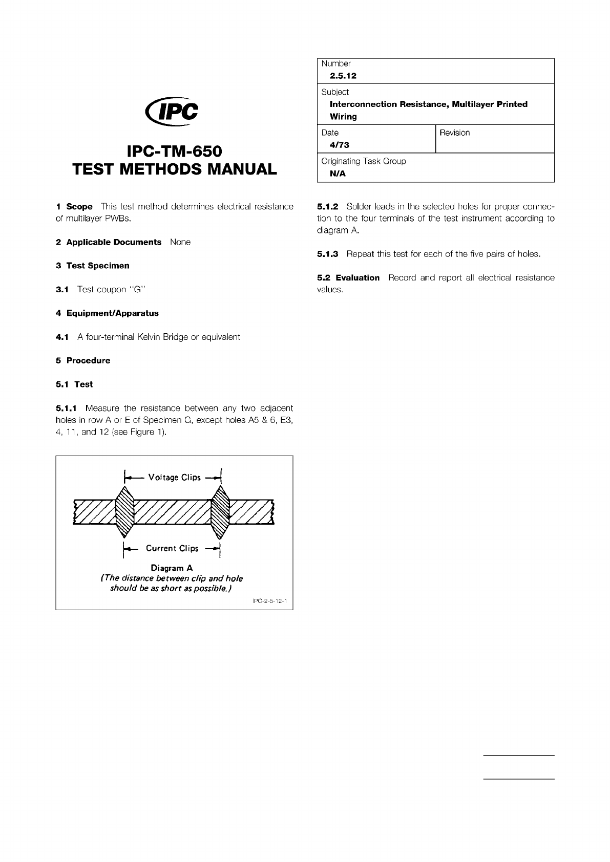
Figure 1 Distance from Clips
The Institute for Interconnecting and Packaging Electronic Circuits
2215 Sanders Road • Northbrook, IL 60062
Material in this Test Methods Manual was voluntarily established by Technical Committees of the IPC. This material is advisory only
and its use or adaptation is entirely voluntary. IPC disclaims all liability of any kind as to the use, application, or adaptation of this
material. Users are also wholly responsible for protecting themselves against all claims or liabilities for patent infringement.
Equipment referenced is for the convenience of the user and does not imply endorsement by the IPC.
Page 1 of 1
回
IPC-TM-650
TEST
METHODS
MANUAL
1
Scope
This
test
method
determines
electrical
resistance
of
multilayer
PWBs.
2
Applicable
Documents
None
3
Test
Specimen
3.1
Test
coupon
"G”
4
Equipment/Apparatus
4.1
A
four-terminal
Kelvin
Bridge
or
equivalent
5
Procedure
5.1
Test
5.1.1
Measure
the
resistance
between
any
two
adjacent
holes
in
row
A
or
E
of
Specimen
G,
except
holes
A5
&
6,
E3,
4,
11
,
and
12
(see
Figure
1).
Diagram
A
(The
distance
between
dip
and
hole
should
be
as
short
as
possible.)
Number
2.5.12
Subject
Interconnection
Resistance,
Multilayer
Printed
Wiring
Date
Revision
4/73
Originating
Task
Group
N/A
5.1.2
Solder
leads
in
the
selected
holes
for
proper
connec¬
tion
to
the
four
terminals
of
the
test
instrument
according
to
diagram
A.
5.1.3
Repeat
this
test
for
each
of
the
five
pairs
of
holes.
5.2
Evaluation
Record
and
report
all
electrical
resistance
values.
I
PC-2-5-1
2-1
interconnects, but a practical issue of operator ability to use
hand-held probes may be considered. Test reports must
report any deviation from the nominal contact land and PTH
geometry.
3.9 Contact Land Pitch
Whenever possible, the center-
to-center distance between the signal and reference lands
of the test interconnect should be consistent to simplify
probing requirements and ensure measurement repeatability
and reproducibility. Nominal center-to-center pitch
be
1.91 mm [0.075 in]. The use of different contact and probe
pitches must be specified and documented.
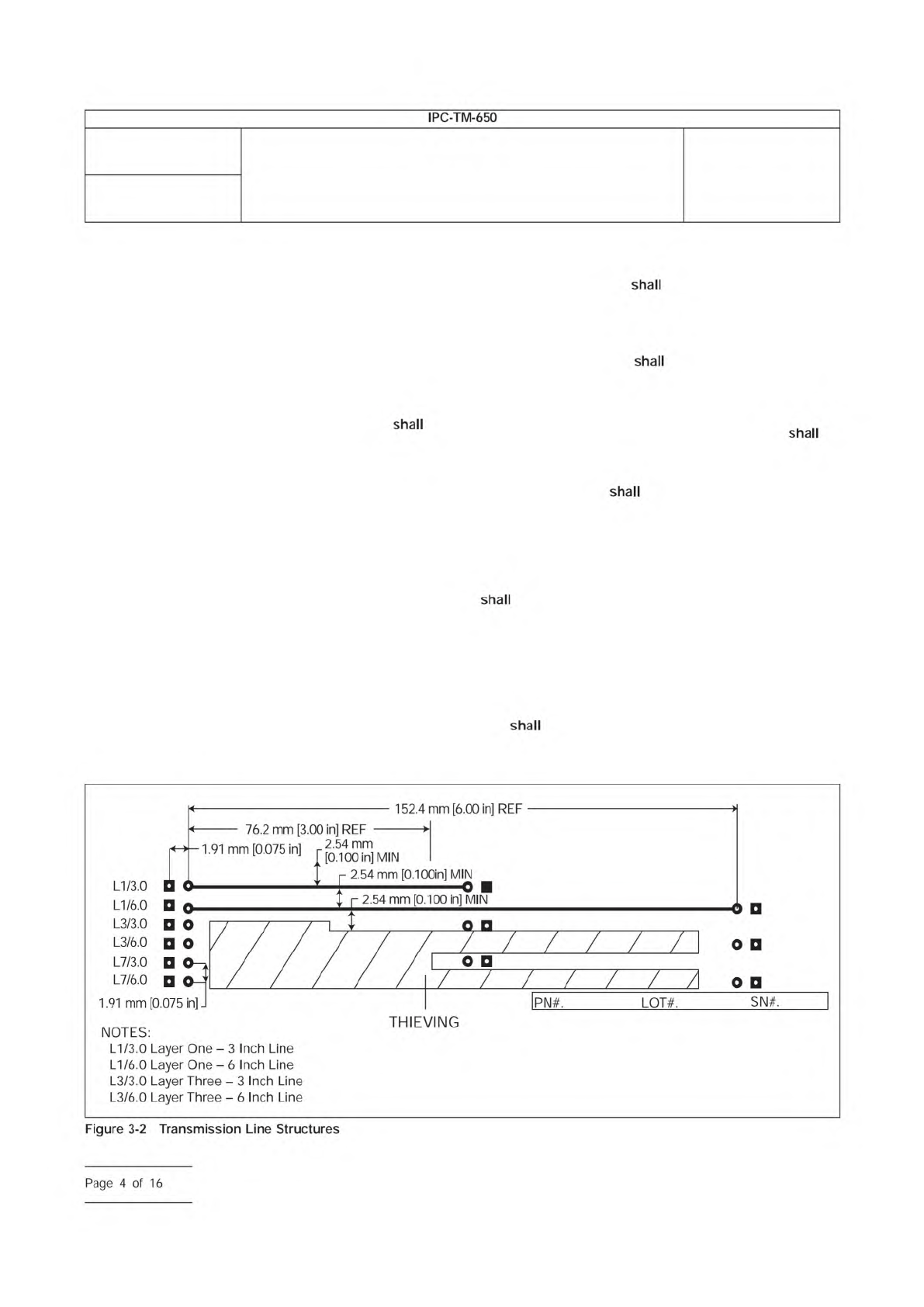
3.10 Single-Signal Conductor Transmission Line
The
single-signal conductor transmission line is also known as the
single-ended, unbalanced, and asymmetrical structure. The
probing area for these lines should consist of a contact land
(see Figure 3-2) for each signal line. The contact land should
provide connection to the reference, or ground, connection for
the test structure. This method requires the use of one con-
tact pitch to ensure measurement consistency between the
test structures of the specimen.
3.11 Orientation
The contact land orientation (placement
and angle of the contact land of the signal line relative to the
contact land of the reference plane) must be the same for all
test interconnects of the specimen in order to ensure mea-
surement consistency between test interconnects.
3.12 Test Interconnect Routing
a. The test interconnects only be routed over and under
contiguous ground and voltage planes following controlled
line impedance guidelines (see IPC-2141). The test inter-
connects must not extend into PTH clearance areas.
b. The test interconnects
be kept at least six times the
width of the signal conductor or 2.5 mm [0.0984 in],
whichever is greater, from any PTHs and any other inter-
connect on the same plane. All conductive material (such
as copper nomenclature, copper thieving, etc.)
be
kept at least 2.5 mm [0.0984 in] from each test intercon-
nect.
c. Test interconnects
be straight or contain gradual and
rounded bends.
3.13 Nomenclature
Labeling of all test interconnect con-
tact lands on at least one surface layer is required for opera-
tor identification during manual probing operations. The label
minimally contain information about which signal layer
the test interconnect is modeling (for example, L1-3in, L1-6in,
etc.). Nomenclature should be etched in copper and be
spaced a minimum of at least six times the width of the signal
conductor (of the test interconnect) or 2.5 mm [0.0984 in],
whichever is greater, from the test interconnect area. When-
ever practical, the terminations at both ends of test intercon-
nect
be marked.
IPC-25511-3-2
Number
2.5.5.11
Subject
Propagation Delay of Lines on Printed Boards by TDR
Date
04/2009
Revision
IPC-TM-650
shall
shall
shall
shall
shall
152.4
mm
[6.00
in]
REF
76.2
mm
[3.00
in]
REF
1.91
mm
[0.075
in]
厂
2.54
mm
[0.100
in]
MIN
2
口
/ /
/
/
/
SN#.
1.91
mm
[0.075
in]-
PN#.
LOT#.
L1/3.0
L1/6.0
L3/3.0
L3/6.0
L7/3.0
L7/6.0
2.54
mm
[0.100
in]
MIN
2.54
mm
[O.IOOin]
MIN
NOTES:
L1/3.0
Layer
One
-
3
Inch
Line
L1/6.0
Layer
One
-
6
Inch
Line
L3/3.0
Layer
Three
-
3
Inch
Line
L3/6.0
Layer
Three
-
6
Inch
Line
THIEVING
Figure
3-2
Transmission
Line
Structures
Page
4
of
16
3.14 Additional Guidelines for Testing Panel Coupons
Test interconnects may be contained within one or more
panel coupons. It is recommended that there be at least one
coupon per PB on the panel as long as it does not adversely
affect panel utilization. With this configuration, the following
additional design guidelines apply. More than one coupon
may be necessary on a PB to ensure uniformity. Also, more
test interconnects may be required than can fit inside one test
coupon. In that case, more than one test coupon is neces-
sary.
3.14.1 Reference and Ground Planes
All reference
planes existing in the coupon are to be connected together
within the coupon area and be electrically independent of con-
ductor planes in the functional circuit area.
3.14.2 Surface Condition
The panel test coupons
have the same surface plating and use the same solder mask
requirements as the functional PB.
3.14.3 Thieving
Differences in circuit density between the
inside of a panel coupon and the functional area may produce
surface plating and etching differences. In order to compen-
sate for these differences, thieving (the use of nonterminated
copper structures, such as planes, pads, and/or traces adja-
cent to test lines) may be used. All thieving structures
be
kept at least six times the width of the signal conductor (of the
test interconnect) or 2.5 mm [0.0984 in], whichever is greater,
from each test interconnect.
4 Apparatus and Instrumentation
The TDR measure-
ment system contains a step generator, a high-speed sam-
pling oscilloscope, and all the necessary accessories for con-
necting the TDR unit to the test structures under test. IPC-
2141 provides a discussion of the TDR system architecture,
system considerations, and the TDR measurement processes
used herein.
4.1 Measurement System Requirements
4.1.1 Voltage Measurement Accuracy
The voltage mea-
surement accuracy and linearity of the TDR sampling oscillo-
scope
be sufficient to provide the required accuracy in
the value of propagation delay. Nominally, the voltage mea-
surement accuracy should be better than ± 1%.
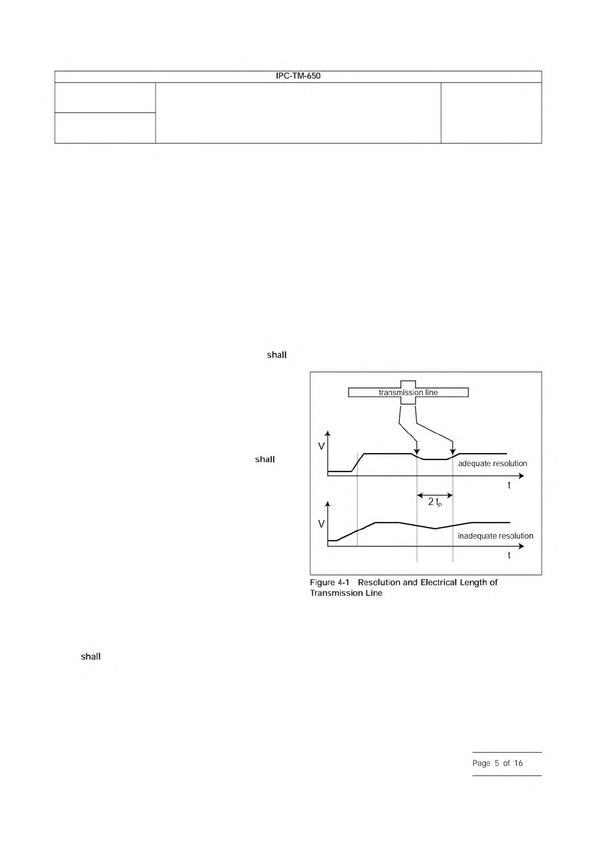
4.1.2 Temporal/Spatial Resolution
The resolution limit of
a given TDR unit is defined as that particular time or distance
wherein two discontinuities or changes on the transmission
line being measured, that would normally be individually dis-
cernable, begin to merge together because of limited TDR
system bandwidth, timing jitter, or a reduced signal-to-noise
ratio. The resolution limit is specified in either time or distance,
and is always related to the one-way propagation time
between the two discontinuities t
P
(see Figure 4-1), and not
the round trip propagation time 2 t
P
.
Per this definition, the temporal resolution limit is:
a. one half of the system risetime, that is 0.5 t
sys
, where t
sys
is the 10 to 90% risetime or 90% to 10% falltime depend-
ing on the propagating edge of the TDR signal;
and the spatial resolution limit is:
b. 0.5 t
sys
x v
p
, where v
p
is the signal propagation velocity in
the transmission line being measured.
For a given length of transmission line to be measured, the
resulting spatial resolution of the TDR measurement set-up
should not exceed one fourth (0.25) of the available length of
the transmission line L
TL
. In other words, L
TL
should be at
least four times the spatial resolution of the measurement sys-
tem.
Table 4-I relates TDR system risetime values to minimum
L
TL
for typical surface microstrip lines in air on FR4 PB mate-
rial (v
p
≈ 2x10
8
m/s).
IPC-25511-4-1
Number
2.5.5.11
Subject
Propagation Delay of Lines on Printed Boards by TDR
Date
04/2009
Revision
IPC-TM-650
shall
shall
Page
5
of
16