IPC-TM-650 EN 2022 试验方法--.pdf - 第524页
Figure 5 Dual Expo sure Picture TD R Trace Figure 6 T est Cable Hookup IPC-TM-650 Number Subject Date Revision Page 3 of 3 2.5.19 Propagation Delay of Flat Cables Using Time Domain Reflectometer 7/84 A IPC-2-5-19-4 — E F…

The transmission line parameters R(f), L(f), C(f), and G(f) are a
consequence of determining α(f) and β(f) from the fitted trans-
mission line solution to the measurements. The final step is
the extraction of the relative dielectric constant ε
r
and loss
tangent, tanδ.
Measurements made of the capacitance and loss tangent of
an additional large parallel plate structure embedded in the
same layer with the signal conductor allows the extraction of
ε
r
and tanδ at very low frequencies. The final R(f), L(f), C(f), and
G(f) are used to extract the complex permittivity using Equa-
tions [1-2] and [1-3].
ε
r
(ω) =
(
C(ω)
C
1MHz
)
x ε
r1MHz
[1-2]
tanδ(ω) =
G(ω)
ωC(ω)
[1-3]
where C
1MHz
is the calculated line capacitance at a low
frequency such as 1 MHz and ε
r1MHz
is the value obtained at
1 MHz from the parallel plate measurement. ω is the angular
frequency and equal to 2πf.
The IPC SPP method is intended for printed boards, however
it can be extended to measure coaxial single-ended and dif-
ferential cables, flex cables, multi-chip module ceramic wiring,
single and multi-chip organic module wiring, thin-film wiring,
and on-chip wiring. The extraction results produce results in
frequency range between 10 KHz to 40 GHz, depending on
the quality of the TDR equipments and test coupon structure.
1.4 SET2DIL (Method D Description)
In this method a
TDR step is injected into one half of a 101.6 mm [4.0 in] dif-
ferential pair, which has the two legs of the differential pair
shorted together at the far end. The waveforms of both halves
of the differential pair are captured and manipulated to derive
SDD21 (and Z
0
, if desired) of the equivalent differential pair.
1.4.1 SET2DIL Measurement System Caveats
SET2DIL
produces the SDD21 value for the differential pair being mea-
sured; it is not intended to rigorously differentiate between
loss elements (conductor vs. dielectric, for instance). The
same structure can also be used to measure the differential
impedance, though that calculation isn’t covered in this speci-
fication. Some other limitations of SET2DIL include:
a) SET2DIL SDD21 measurements will include losses due to
the vias, for stripline traces. To minimize errors induced by
vias, the following limitations are made to the SET2DIL
coupon design:
i. The coupon has an effective length of 203.2 [8.0 in],
which will cause the trace losses to overwhelm small via
losses.
ii. Stripline traces on the bottom portion of the board
(lower layers) are measured from the top to minimize
via stub effects. Upper stripline layers are measured
from the bottom of the board.
b) SET2DIL SDD21 measurements will include an error term
from SDD11 effects if the differential trace being measured
isn’t 100 Ω (2x the reference impedance of 50 Ω).
i. The coupon has an effective length of 203.2 mm [8.0 in],
causing the trace insertion losses (SDD21) to overwhelm
the relatively small return loss.
ii. The primary purpose of SET2DIL is to ensure the trace
properties match that of those in simulations. Thus,
SDD21 from simulations with a 50 Ω reference can be
used as the measurement criteria for SET2DIL, making
the reference error difference moot.
1.5 FD (Method E Description)
Three of the previously
described methods use TDR to determine the loss character-
istics of a printed board. This approach utilizes a Vector Net-
work Analyzer (VNA) or the fast fourier transform (FFT) of a
TDT for this purpose. The result is a direct measure of fre-
quency domain attenuation and loss. VNA equipment includes
calibration to the launch pad which must be used. The inser-
tion loss is directly related to transmission line design param-
eters utilized in signaling design analysis. The metric for the FD
method is the slope of the RMS insertion loss fit for a speci-
fied frequency range.
2 APPLICABLE DOCUMENTS
Controlled Impedance Circuit Boards and High
Speed Logic Design
Test Methods Manual
1.9 Measurement Precision Estimation for Variables Data
2.5.5.7 Characteristic Impedance of Lines on Printed Boards
by TDR
Annex 69b.4.1, ‘‘Fitted attenuation’’
2.1 Technical Publications
R. Mellitz, T. Ballou, and S.G. Pytel, ‘‘Energy Based TDR Loss
Method for PB Manufacturers,’’ from IPCWorks 2005, Las
Vegas, NV.
Number
2.5.5.12
Subject
Test Methods to Determine the Amount of Signal Loss on
Printed Boards
Date
07/12
Revision
A
IPC-TM-650
IPC-2141
IPC-TM-650
IEEE802.3ap
Std
2007
Page
3
of
24
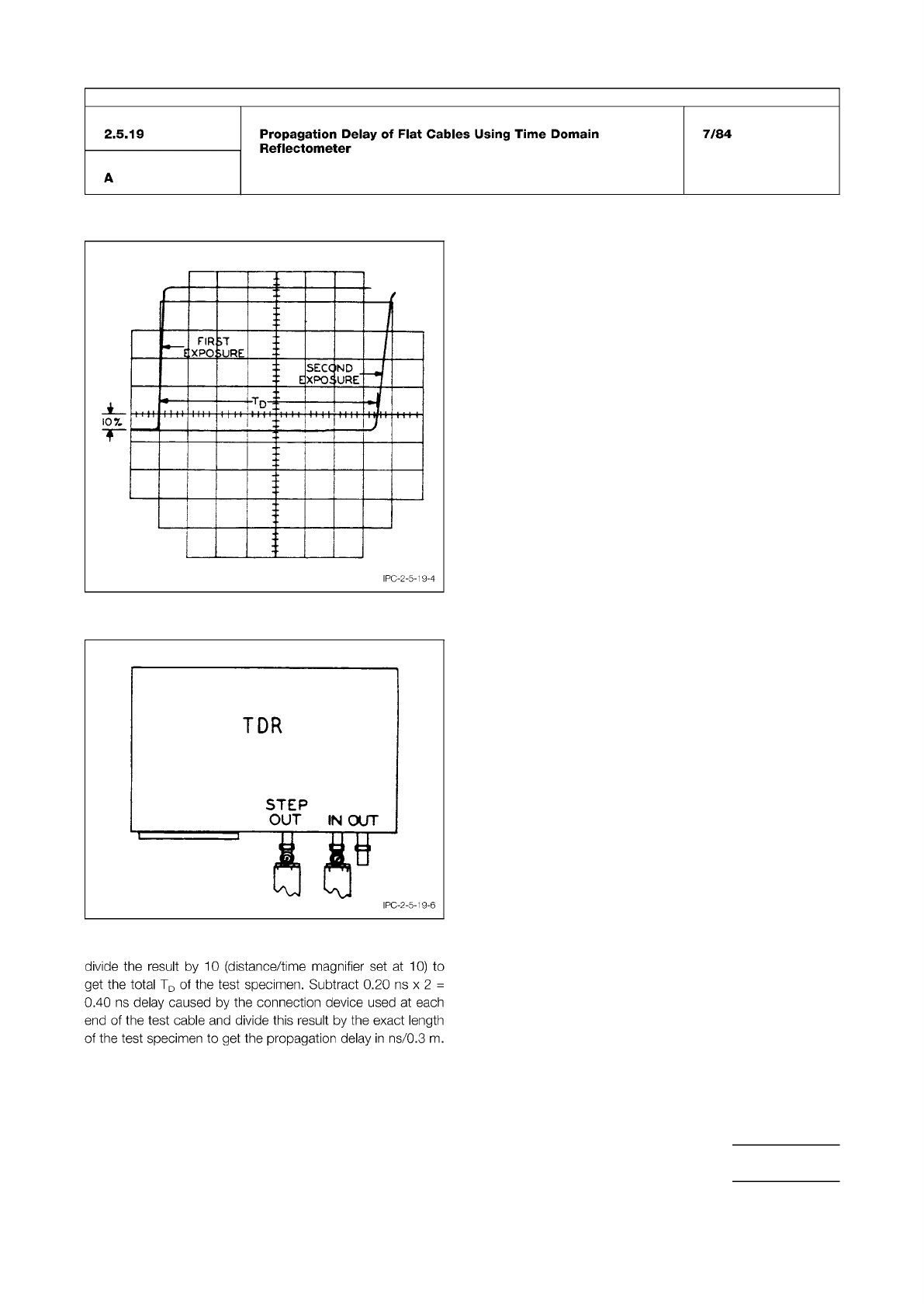
Figure 5 Dual Exposure Picture TDR Trace
Figure 6 Test Cable Hookup
IPC-TM-650
Number
Subject Date
Revision
Page 3 of 3
2.5.19
Propagation
Delay
of
Flat
Cables
Using
Time
Domain
Reflectometer
7/84
A
IPC-2-5-19-4
—
E
FIR
XPQ
ARE
7
:
E
SECC
XPOE
ND
URE”
i
-
i
l
-Tn
・
j
•一一
1111
1
1
1
1
f
>
f
!
”11
t t
t
t
TDR
STEP
OUT
IN
OUT
I
PC-2-5-1
9-6
divide
the
result
by
10
(distance/time
magnifier
set
at
10)
to
get
the
total
TD
of
the
test
specimen.
Subtract
0.20
ns
x
2
=
0.40
ns
delay
caused
by
the
connection
device
used
at
each
end
of
the
test
cable
and
divide
this
result
by
the
exact
length
of
the
test
specimen
to
get
the
propagation
delay
in
ns/0.3
m.
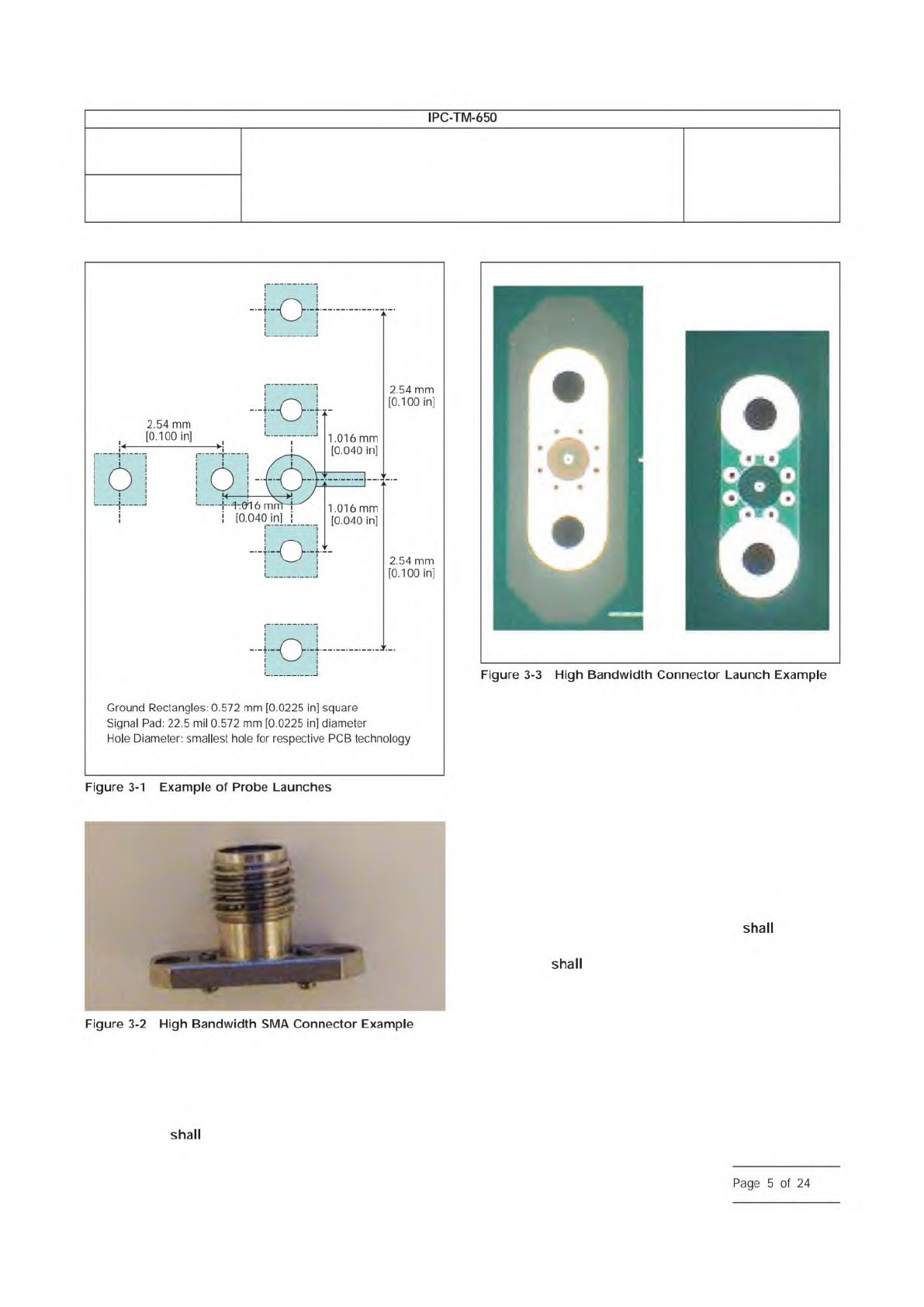
3.1.7 General Thieving
Thieving which is the use of
nonterminated copper structures, such as planes, pads,
and/or conductors adjacent to test lines that ensure plating
consistency may be used on test coupon. All thieving struc-
tures, if used,
be placed at least six times the width of
the signal conductor (of the test interconnect) or 2.5 mm
[0.100 in], whichever is greater, from each test interconnect.
3.1.8 Termination Types of Test Lines
There are two
types of line styles that may be used. The first is terminated on
each end with a launch. These lines are the only type that are
employed with the SPP and VNA method. The second type of
line is terminated on one end with a launch while the other end
is just the end of a conductor e.g., unterminated. The EBW
and RIE method may use either terminated or unterminated
lines types. The SET2DIL structure requires no termination.
3.1.9 Test Line Routing
The test lines be routed
over/under contiguous ground/voltage planes. The test line
conductors
be kept at least six times the height of the
laminate layer thickness which is closest to the conductor or
2.54 mm [0.100 in], whichever is greater; from printed board
structures include voids, plane splits, other conductors, and
holes.
It is recommended that test lines be straight.
3.1.10 Environmental Conditioning: Temperature and
Humidity
Temperature and humidity effect loss measure-
ments. Consistent results can be obtained by storing test
IPC-25512-3-1
IPC-25512-3-3
Number
2.5.5.12
Subject
Test Methods to Determine the Amount of Signal Loss on
Printed Boards
Date
07/12
Revision
A
IPC-TM-650
—
Ground
Rectangles:
0.572
mm
[0.0225
in]
square
Signal
Pad:
22.5
mil
0.572
mm
[0.0225
in]
diameter
Hole
Diameter:
smallest
hole
for
respective
PCB
technology
Figure
3-1
Example
of
Probe
Launches
Figure
3-2
High
Bandwidth
SMA
Connector
Example
Figure
3-3
High
Bandwidth
Connector
Launch
Example
shall
shall
Page
5
of
24