IPC-TM-650 EN 2022 试验方法--.pdf - 第549页
1 Scope and Purpose 1.1 Sco pe This do cument describes the frequency domain test methods to a ccurately determine the amount of signal propagation loss and delay f or electrical printed boards, to meet the demand of hig…

1 Scope
The fungus resistance test is used to determine
the resistance of materials to fungi and to determine if such
material is adversely affected by fungi under conditions favor-
able for their development, namely high humidity, warm atmo-
sphere, and presence of inorganic salts.
2 Applicable Documents
None
3 Test Specimen
Specimens must be a minimum size of
50 mm x 50 mm [1.97 in x 1.97 in] with copper foil (if appli-
cable) removed by etching using standard commercial prac-
tices.
4 Apparatus and Reagents
4.1 Test Chamber
The incubator shall be capable of main-
taining 30 ± 1 °C [86 ± 2 °F] and 95 ± 2% relative humidity
and have an ultraviolet (360 nm) source for subsequent
decontamination. Provisions shall be made to prevent con-
densation from dripping on the test item. There shall be free
circulation of air around the test item and the contact area of
fixtures supporting the test item shall be kept to a minimum.
4.2 Sterilizer
4.3 Centrifuge
4.4 pH Meter
4.5 Colony Counter
4.6 Incubator
4.7 Dishwasher
4.8 Petri Dishes
4.9 Filter Paper
4.10 Media Solutions
4.11 Microorganisms
4.12 Atomizer, 15,000 ± 3000 spores
5 Procedures
5.1 Preparation of Test Media
5.1.1 Mineral-Salts Solution
Prepare the solution to contain the following:
Potassium dihydrogen orthophosphate (KH
2
PO
4
) .......... 0.7g
Potassium monohydrogen orthophosphate (K
2
HPO
4
) ... 0.7g
Magnesium sulfate heptahydrate (MgSO
4
c7H
2
O) ........... 0.7g
Ammonium Nitrate (NH
4
NO
3
) ......................................... 1.0g
Sodium chloride (NaCl) .............................................. 0.005g
Ferrous sulfate heptahydrate (FeSO
4
c7H
2
O) ............... 0.002g
Zinc sulfate heptahydrate (ZnSO
4
c7H
2
O) .................... 0.002g
Manganous sulfate monohydrate (MnSO
4
cH
2
O) ......... 0.001g
Distilled water ........................................................... 1000 ml
Sterilize the mineral salt solution by incubating at 121 °C [250
°F] for a minimum of 20 minutes. Adjust the pH of the solution
by the addition of 0.01 normal solution of NaOH so that after
sterilization the pH is between 6.0 and 6.5. Prepare sufficient
salt solutions for the required tests.
5.1.2 Purity of Reagents
Reagent grade chemicals shall
be used in all tests. Unless otherwise specified, it is intended
that all reagents shall conform to the specification of the Com-
mittee on Analytical Reagents of the American Chemical Soci-
ety, where such specifications are available.
5.1.3 Purity of Water
Unless otherwise specified, refer-
ences to water shall be understood to mean distilled water or
water of equal purity.
5.1.4 Preparation of Mixed Spore Suspension
The following test fungi shall be used:
Description .................................................................. ATCC
Aspergillus niger ............................................................ 9642
Chaetomium globosum ................................................. 6205
Gliocladium virens ......................................................... 9645
Aureobasidium pullulans ............................................... 9348
Penicillium funiculosum ................................................. 9644
5.1.5
Maintain cultures of these fungi separately on an
appropriate medium such as potato dextrose agar. However,
the culture of Chaetomium globosum shall be cultured on
3000 Lakeside Drive, Suite 309S
Bannockburn, IL 60015-1249
IPC-TM-650
TEST METHODS MANUAL
Number
2.6.1
Subject
Fungus Resistance of Printed Board Materials
Date
03/07
Revision
G
Originating Task Group
Solder Mask Performance Task Group (5-33b)
ASSOCIATION CONNECTING
ELECTRONICS INDUSTRIES
®
Material
/n
this
Test
Methods
Manual
was
voluntarily
established
by
Technical
Committees
of
I
PC.
This
material
/s
advisory
only
and
"s
use
or
adaptation
,
s
entirely
voluntary.
IPC
disclaims
all
liability
of
any
kind
as
to
the
use,
application,
or
adaptation
of
this
material.
Users
are
also
wholly
responsible
for
protecting
themselves
against
all
claims
or
liabilities
for
patent
infringement.
Equipment
referenced
/s
for
the
convenience
of
the
user
and
does
not
imply
endorsement
by
IPC.
Page
1
of
3
1 Scope and Purpose
1.1 Scope
This document describes the frequency domain
test methods to accurately determine the amount of signal
propagation loss and delay for electrical printed boards, to
meet the demand of high speed applications nowadays. As
the data rate of high speed IO continues to increase (e.g., 10
Gbps and above), production testing and development testing
require more precise and accurate high frequency methods.
(Existing IPC-TM-650 Test Methods such as Method
2.5.5.12A are not adequate). Additionally, previous IPC test
methods do not encompass traditional industry methods
using VNA, such as thru-reflect-line (TRL), and recent devel-
opments of 2X-Thru test methods, etc. This test method is
defined to close the gaps.
The scope of this test method includes:
• Calibration and/or de-embedding techniques
• Probing/test fixture choices that impact measurement
quality
• Coupon Design
• Test sample pre-conditioning
• Environmental impact, etc.
1.2 Purpose
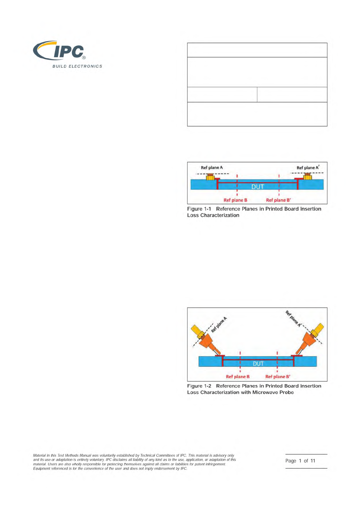
1.2.1 The importance of Setting up Correct Reference
Plane for Printed Board Characterization
The impor-
tance of setting up a correct reference plane in a typical inter-
connect measurement setup is illustrated in Figure 1-1. The
vector network analyzer (VNA) has been the de-facto standard
for accurate passive interconnect characterization including
the printed circuit board, connector, cables, etc. Making high
quality VNA measurement is straight-forward with standard
coaxial connectors and precision SOLT (short, open, load,
through) calibration kits. However, test fixtures are usually
required to connect the standard coaxial connectors to the
non-coaxial device under test (DUT). SOLT calibration can
readily move the reference plane to Ref plane A and Ref plane
A’ in the figure, while the intended DUT is the printed board
conductor only (between Ref plane B and Ref plane B’). The
test fixtures (between A and B, A’ and B’) need to be charac-
terized and then de-embedded to recover the insertion loss of
DUT.
Microwave probes are often used to probe interconnect struc-
tures for quick measurement, as shown Figure 1-2. A similar
calibration or de-embedding procedure is needed to move the
reference plane to the target location (Ref plane B and B’
shown in the figure). Note that sometimes, an SOLT calibra-
tion procedure can be carried out using calibration substrates
provided by probe vendor, to move the reference plane to the
probe tip, but it does not move the reference plane to the tar-
get location and additional de-embedding procedure is still
needed.
In a general calibration/de-embedding process, specialized
calibration standards with known electrical properties are
inserted at the end of the test fixture, and a calibration pro-
cess is performed to move the reference plane to the end of
IPC-25514-1-1
IPC-25514-1-2
3000 Lakeside Drive, Suite 105N
Bannockburn, IL 60015-1249
IPC-TM-650
TEST METHODS MANUAL
Number
2.5.5.14
Subject
Measuring High Frequency Signal Loss and
Propagation on Printed Boards with Frequency
Domain Methods
Date
02/2021
Revision
Originating Task Group
High Frequency Signal Loss Test Methods Task
Group (D-24D)
C/PC@
BUILD
ELECTRONICS
Ref
plane
A
Ref
plane
A’
Ref
plane
B
Ref
plane
B'
Figure
1-1
Reference
Planes
in
Printed
Board
Insertion
Loss
Characterization
Ref
plane
B
Ref
plane
B*
Figure
1-2
Reference
Planes
in
Printed
Board
Insertion
Loss
Characterization
with
Microwave
Probe
Material
/n
this
Test
Methods
Manual
was
voluntarily
established
by
Technical
Committees
of
I
PC.
This
material
/s
advisory
only
and
"s
use
or
adaptation
,
s
entirely
voluntary.
IPC
disclaims
all
liability
of
any
kind
as
to
the
use,
application,
or
adaptation
of
this
material.
Users
are
also
wholly
responsible
for
protecting
themselves
against
all
claims
or
liabilities
for
patent
infringement.
Equipment
referenced
/s
for
the
convenience
of
the
user
and
does
not
imply
endorsement
by
IPC.
Page
1
of
11
the test fixture. The accuracy of the measurement relies highly
on the quality of the physical calibration standards, especially
for SOLT type of calibration standards, where the parasitics of
the SOLT calibration standard must be known a priori. How-
ever, for printed board structures, it is not feasible to build an
accurate broadband SOLT structure right after the test fixture.
Hence the on-board SOLT calibration process usually does
not work well above a few GHz.
There are existing calibration/de-embedding methods in the
industry for general purpose interconnect characterization to
move the calibration reference plane from the coaxial connec-
tor to printed board interfaces. These methods are proven by
the industry and are applicable to printed board characteriza-
tion as well. Two of such methods are outlined in 1.3.1 and
1.3.2. However, for the accurate characterization of propaga-
tion constant of the uniform transmission line section, simpler
and more universal technique can be used as outlined in
1.2.2.
1.2.2 Eigenvalue based De-embedding Methodology for
Printed Board Trace Insertion Loss Measurement
For
printed board trace characterization, there are simple
approaches to derive the printed board insertion loss, when
the DUT is a uniform transmission line. There are multiple pub-
lications proposed that using T-matrix of an ideal transmission
line segment can significantly simplify the de-embedding algo-
rithm. The T-matrix is diagonal exponential in the modal space
when normalized to the modal characteristic impedance of the
transmission line [1]-[6]. If T-matrix of a multi-conductor line
segment is converted to S-matrix, the result is an
S-parameters (where reference impedance is defined as the
characteristic impedance of the transmission line):
S
DUT
=
[
0
e
−γ L
e
−γ L
0
]
(Eq.1)
where γ is the complex propagation constant, and L the line
length. An eigenvalue based de-embedding procedure can be
carried out utilizing the above assumptions, by measuring S
parameters of two different routing lengths. There are various
(similar) derivations procedures, and below is one example:
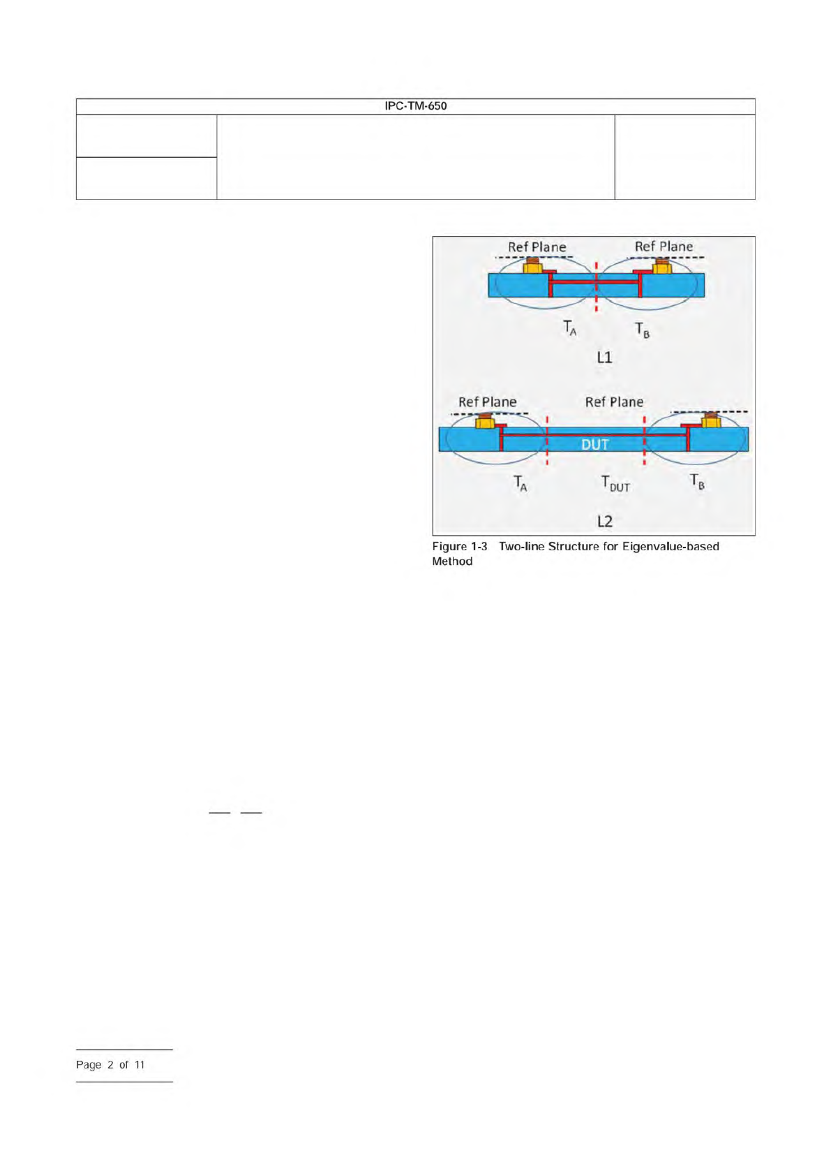
In Figure 1-3, two printed board conductors with different
lengths (L1 and L2) are fabricated on the same test coupon.
If we pick the mid-point of L1 structure, and use T-matrices to
describe the network parameter of left and right portion of the
structure as T
A
and T
B
, then we have
T
L1
= T
A
x T
B
(Eq. 2)
T
L2
= T
A
x T
DUT
x T
B
(Eq. 3)
where DUT is the transmission line with length of L2-L1. From
(1) and (2) we can easily get
T
L2
x T
L1
-1
= T
A
x T
DUT
x T
B
x T
B
-1
x T
A
-1
= T
A
x T
DUT
x T
A
-1
(Eq. 4)
Therefore, T
L2
x T
L1
-1
and T
DUT
are similar matrices and should
have the same eigenvalue. Meanwhile, assuming the DUT is a
uniform transmission line, we have:
T
DUT
=
[
e
γ (L2-L1)
0
0
e
−γ (L2-L1)
]
(Eq.5)
Where γ is the complex propagation constant of the trans-
mission line. There are two eigenvalues of the matrix
T
L2
x T
L1
-1
(the two non-zero diagonal terms in equation 4),
where the one with absolute value <1 is the printed board
conductor loss corresponding to the routing length of (L2-L1).
Once the eigenvalue is identified, the insertion loss is readily
IPC-25514-1-3
Number
2.5.5.14
Subject
Measuring High Frequency Signal Loss and Propagation on
Printed Boards with Frequency Domain Methods
Date
02/2021
Revision
IPC-TM-650
Figure
1-3
Two-line
Structure
for
Eigenvalue-based
Method
Page
2
of
11