IPC-TM-650 EN 2022 试验方法--.pdf - 第554页
As the solid metal p lanes may block the moisture p enetr a tion, for the conductors routed on inner layers it typically takes a long time (with rare exceptio ns) for the sa mple to absorb the moisture. Therefore, making…
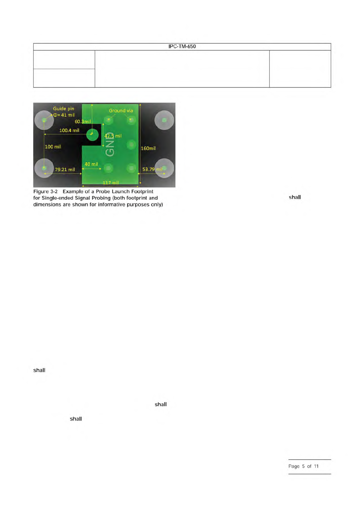
It is important to note that these are just footprint examples,
and the electrical performance of these footprint may be fur-
ther improved based on the layer stackup, such as voiding the
ground plane right beneath the signal pads. Each probe ven-
dor can specify its optimized probe launch footprint that
meets the electrical requirement specified in 4.2. Furthermore,
it is critical to work with probe vendor to make sure the fin-
ished drill hole size is compatible with the probe.
Note that the footprint example shown in Figure 3-1 is appli-
cable for measurements up to 20GHz and that the footprint
can be further optimized for application at higher frequencies.
3.4 Connector Launch
Alternative to microwave probes,
high bandwidth connector launch may be used instead of
probe launch as show in Figure 3-2 and Figure 3-3 of IPC-
TM-650 Method 2.2.2.12A. Although the hand-held probe
approach is quicker and more convenient to use, the connec-
tor solution is usually more reliable and less prone to human
errors.
3.5 General Surface Condition
The panel test coupons
have the same surface plating and use the same solder
mask requirements as the functional printed board. The plat-
ing of the launch footprint should be suitable for probing or
co-axial connector connection.
3.6 General Routing Guidelines
The test lines be
referenced to a continuous ground/voltage planes. The test
line conductors
be kept at minimum distance Dmin from
printed board structures such as voids, plane splits, other
conductors and holes, where Dmin is six times the height of
dielectric layer (from line conductor to the closest reference
plane) or 2.54 mm [0.100 in], whichever is greater.
Fiber-weave impact should be mitigated unless the intent is to
measure its impact. One mitigation example is to have the test
line routed at about 10 degree angle (or close to the routing
scenario in actual product design) with respect to the fiber-
weave alignment. Alternative, straight routing (parallel to board
edge) can be used if the Gerber image is rotated by about 10
degrees on the panel.
It is recommended to route the test lines with the same cross-
section and target impedance as in the actual product layout.
Thieving, which is the use of non-terminated copper struc-
tures such as planes, pads, and/or conductors adjacent to
test lines that ensure plating consistency, may be used on the
test coupon. All thieving structures (if used)
be placed at
least Dmin away from each test interconnect. It is recom-
mended to make sure copper density at each routing layer is
representative of the actual product.
3.7 Impact of Vias in the Printed Board Conductor Loss
Characterization
Measuring the signal loss for inner layer
(stripline) can be challenging when there is a substantial loss
due to the via or via stub effect. Reducing via effect can
improve the de-embedding results. This can be achieved by:
• Minimizing via stub length by probing from the appropriate
side of the board (from the top for traces on the bottom half
of the board and vice-versa, to assure minimum via stub
length)
• Minimizing via stub length by back-drilling. However, this
needs to be done with good control of back-drilling depth.
Inconsistent back-drilling depth between the vias for two
different routing length can lead to large de-embedding error
• Extra attention needs to be paid to stacked via designs, as
this approach, while avoiding stubs and improving signal
integrity, has high manufacturing variants
• The resonance frequency should be outside of intended
measurement bandwidth
For signals on outer layer (microstrip), the conductor should
be routed without via or via stub.
3.8 Impact of Environmental Condition in the Printed
Board Conductor Loss Characterization
Temperature
and humidity affect loss measurements. It is therefore critical
to clearly document the testing condition in the reported inser-
tion loss.
For insertion loss of conductors routed on outer layer, the
results can be different under the conditions described in
3.8.1 vs. those described in 3.8.2 due to the humidity impact.
IPC-25514-3-2
Number
2.5.5.14
Subject
Measuring High Frequency Signal Loss and Propagation on
Printed Boards with Frequency Domain Methods
Date
02/2021
Revision
IPC-TM-650
—
Figure
3-2
Example
of
a
Probe
Launch
Footprint
for
Single-ended
Signal
Probing
(both
footprint
and
shall
dimensions
are
shown
for
informative
purposes
only)
shall
shall
shall
Page
5
of
11
As the solid metal planes may block the moisture penetration,
for the conductors routed on inner layers it typically takes a
long time (with rare exceptions) for the sample to absorb the
moisture. Therefore, making measurement of insertion loss of
inner routing layers under the conditions described in 3.8.1 is
recommended over making such measurements under the
conditions described in 3.8.2.
3.8.1 Insertion Loss Measurement of Vacuumized Test
Specimens
Test specimens can be vacuumized right after
baking them at 105 °C RH 0% over 2 hours, or 140 °C RH
0% over 1 hour. However, if the coupon has been stored over
a long period of time without proper vacuum packaging, the
baking condition needs to be adjusted to be 140 °C RH 0%
for 12 hours. Consistent results can be obtained by testing
specimens at 23 °C (± 2 °C) [73.4 °F (± 3.6 °F)] and 20~80%
RH for less than 12 hours since opening the vacuum package
or finishing a baking treatment. It is recommended to allow
test coupons to cool to room temperature for at least 30 min-
utes before test if measurement is done after a baking treat-
ment.
3.8.2 Insertion Loss Measurement of Test Specimens
Stored in Environmental Chamber
For conductors routed
on outer layers, consistent results of insertion loss at typical
humidity condition can also be obtained by storing test speci-
mens at 23 °C (± 2 °C) [73.4 °F (± 3.6 °F)] and 40% RH (± 5%
RH) for no less than 48 hours. Note that the test under this
condition takes longer time compared to that described in
3.8.1.
4 Apparatus
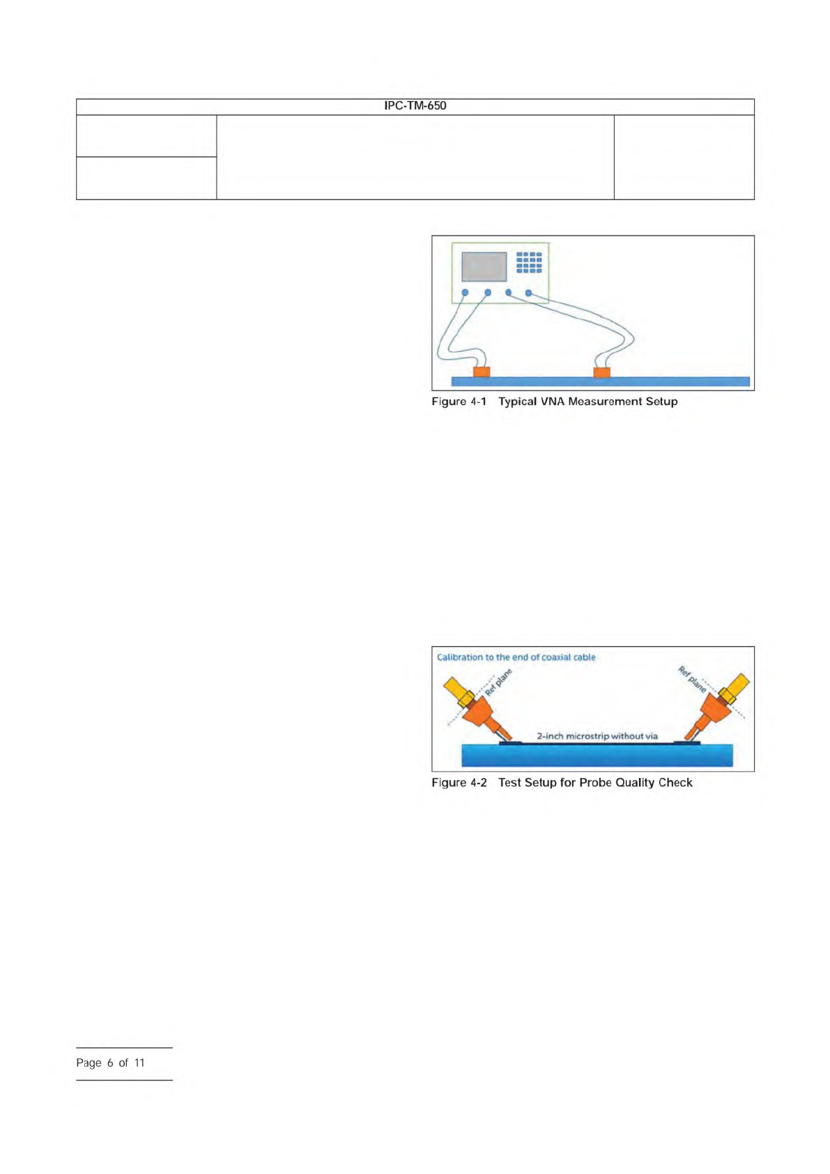
4.1 VNA Measurement Apparatus
The measurement
equipment needed includes a VNA, calibration kit, cabling,
and a probing solution, as shown in Figure 4-1. High perfor-
mance connectors and cables that are rated above the maxi-
mum frequency of interest are required in performing VNA
measurements.
Using TDR/TDT system in place of a VNA to acquire fre-
quency domain attenuation and loss data is beyond the scope
of this test method. A future IPC-TM-650 Test Method
2.5.5.15 for best design practices for Time Domain method is
envisioned under the IPC D-24D Task Group.
4.2 Probe Quality
The quality of probe (whether using
probing station or handheld probe) is critical for accurate and
repeatable measurement. It is recommended to have the
insertion loss of the probe and launching pad to be less than
3.5 dB at highest frequency of interest, to make sure the
probe and launching pad design have good electrical perfor-
mance.
A direct measurement of electrical performance of probe and
launching pad can be cumbersome. Alternatively, Figure 4-2
shows an example of test setup to check the electrical perfor-
mance. A 50.8 mm [2.0 in] microstrip line with known insertion
loss is used to provide a connection between two probes.
VNA is calibrated to the end of coaxial cable, and the inser-
tion loss of the 50.8 mm [2.0 in] microstrip line with probes at
both ends is measured.
Insertion loss requirement for the test setup in Figure 4-2
depends on the highest measurement frequency, as well as
the microstrip trace loss. A test coupon with known loss can
be used, or a separate measurement can be done to deter-
mine microstrip loss. Figure 4-3 shows an example of the
probe quality requirement, assuming the highest measure-
ment frequency is 20 GHz, and the insertion loss of the
50.8 mm [2.0 in] microstrip is 5 dB at 20 GHz. The measured
insertion loss must be above the red dash line in the figure.
Note at DC level, the required loss is less than 1 dB, and at
20 GHz, the required loss is less than12 dB (where 3.5 dB is
allocated for each probe, and 5 dB is coming from the
50.8 mm [2.0 in] microstrip).
IPC-25514-4-1
IPC-25514-4-2
Number
2.5.5.14
Subject
Measuring High Frequency Signal Loss and Propagation on
Printed Boards with Frequency Domain Methods
Date
02/2021
Revision
IPC-TM-650
Calibration
to
the
end
of
coaxial
cable
Figure
4-2
Test
Setup
for
Probe
Quality
Check
Page
6
of
11
Probe performance may degrade over time. It is necessary to
periodically check the probe quality to assure the electrical
requirement in Figure 4-3 is met.
5 Procedure
The procedure section is to be used to detail
all of the specific steps necessary to perform the actual test.
It
include any specific conditioning requirements, or
other specimen preparation not previously detailed. It
then describe in detail the successive steps of the procedure,
grouping related operations into logical divisions in a concise
manner. It
include times, temperatures, voltages, pres-
sures, concentrations, linear measurements and quantitative
criteria when necessary in applicable units (both Metric and
English).
It
then state any detailed information required in report-
ing the test results. When two or more procedures are
described in the same test method, the report
indicate
which of the procedures was used. When a test method
allows variations in operating or other conditions, the report
state the particular conditions utilized for the test.
This specification currently outlines measuring Frequency
Domain characteristics using a VNA.
5.1 VNA Settings
Follow the VNA manual for proper
operation of equipment. Recommended settings for the VNA
include an IF bandwidth of 1 kHz (can be decreased based on
instrument and applications), and a step size of 10 MHz.
Smoothing is not allowed.
The cables and connectors used in the measurement should
be sufficiently rated for the maximum intended measurement
frequency.
5.2 Conditioning of Test Sample
Refer to 3.8 for proper
conditioning of test sample before test.
5.3 VNA Calibration and De-embedding
Calibration
and/or de-embedding techniques outlined in 1.2.1 must be
performed to remove the effects of cable, connector, and test
fixtures.
5.4 Smoothing and Fitting of Insertion Loss Measure-
ment Curve
5.4.1 Insertion Loss Smoothing Basics
Printed board
testing facilities often report insertion loss per inch at a hand-
ful of frequencies (e.g., 4 GHz, 8 GHz, 12.89 GHz, etc.). An
ideal insertion loss curve for a printed board conductor is
expected to follow transmission line behavior and be smooth.
However, in some testing houses, the de-embedded insertion
loss curves may have oscillations and deviations due to vari-
ous sources of measurement and de-embedding error, as
shown in blue curve in Figure 5-1. Without proper post-
processing of the data, the measurement house can easily fail
to report the true loss performance of the test coupon at des-
ignated frequencies. One common methodology for obtaining
a smooth de-embedded insertion loss curve is to use an iter-
ated moving average. The result is a very smooth red curve
shown in Figure 5-1.
While smoothing with an iterative moving average addresses
most of the challenges posed by the measurement errors,
there remain some disadvantages. The resulting smooth curve
is non-physical and unlikely to be representative of the true
loss of printed board conductor. For example, the smoothed
curve usually deviates from the correct answer at low
IPC-25514-4-3
IPC-25514-5-1
Red denotes the smoothed curve
Number
2.5.5.14
Subject
Measuring High Frequency Signal Loss and Propagation on
Printed Boards with Frequency Domain Methods
Date
02/2021
Revision
0
0
5
10
15
20
Frequency
(GHz)
Frequency(GHz)
Figure
4-3
Insertion
Loss
Requirement
for
the
Probe
Quality
Test
Setup
in
Figure
4-2
shall
shall
shall
shall
shall
shall
Figure
5-1
An
Iterative
Moving
Average
Applied
to
a
Typical
Insertion
Loss
Curve
Note
1.
IPC-TM-650
—
3
5
2
5
1
5
N
1
.
6
m
p)
q
o
u-
sso.
(8P)
sso
J
uo
Sil-
Page
7
of
11