IPC-TM-650 EN 2022 试验方法--.pdf - 第569页
IPC-TM-650 Number Subject Date Revision Page 3 of 3 2.5.6 Dielectric Breakdown of Rigid Printed Wiring Material 5/86 B 6.1 The dielectric breakdown of the material may be adversely affected if the drilling process used t…
1 Scope and Purpose
1.1 Scope
This method subjects unpopulated test speci-
mens (samples) to sudden, extreme changes in temperature
in order to evaluate the quality of interconnects formed during
the manufacturing processes.
1.2 Purpose
This method be used to simulate the
thermodynamic effects of extreme temperature variations. The
use of this method is intended to be able to capture ‘‘infant
mortality’’ types of manufacturing defects.
1.2.1
This method may provide for qualification, quality con-
formance testing and lot acceptance.
2 Applicable Documents
Terms and Definitions
Generic Standard on Printed Board Design
Acceptability of Printed Boards
Standard for Printed Board Handling and Storage
Specification for Base Materials for Rigid and Mul-
tilayer Printed Boards
Specification for Base Materials for High Speed/
High Frequency Applications
Qualification and Performance Specification for
Rigid Printed Boards
Qualification and Performance Specification for
Flexible Printed Boards
Qualification and Performance Specification for
High Frequency (Microwave) Printed Boards
Guidelines for Microsection Preparation
Test Methods Manual
1
2.1.1 Microsectioning - Microsectioning, Manual and Semi
or Automatic Method
2.6.27 Assembly Simulation - Thermal Stress, Convection
Reflow Assembly Simulation
3 Terms and Definitions
3.1 Thermal Shock (Unpopulated Printed Board)
A tem-
perature cycle with a change rate of 1 °C or more per second
as measured on the surface of the test specimen, for at least
the center 60% of each transition, during the heating and
cooling portions.
3.2 Thermal Cycle (Unpopulated Printed Board)
A tem-
perature cycle that has a sample change rate of less than 1 °C
per second as measured on the surface of the test specimen,
for at least the center 60% of each transition, during the heat-
ing and cooling portions. While no minimum temperature
change rate is specified, a change rate of at least 10 °C per
minute is expected for qualification testing.
4 Test Specimen
4.1 Design/Construction Criteria
4.1.1
The test specimen be the D coupon in accor-
dance with the requirements of IPC-2221 Appendix A, or
alternate coupon(s) AABUS.
4.1.2
The test specimen(s) be constructed with holes
contained in the printed board it represents as follows:
• Through holes: D coupons
be constructed with both
the largest plated-through holes (PTHs) and the smallest
plated-through vias.
• Propagated structures: D coupons
be constructed
with and represent all applicable blind, buried, or filled
through hole (propagated) via structures as defined in IPC-
2221 Appendix A. D coupons contain two nets (structures).
Multiple D coupons are used for designs with more than two
structures.
4.1.2.1
The test specimen(s) contain the representa-
tive ground and power planes of the printed board design.
4.1.3
The test specimen(s) allow for microsection
evaluation of all the applicable, representative PTHs and vias
defined in 4.1.2 after exposure to the conditions of this Test
Method. IPC-9241 provides guidance on the proper prepara-
tion of a metallographic sample (microsection) of a printed
board.
3000 Lakeside Drive, Suite 105N
Bannockburn, IL 60015-1249
IPC-TM-650
TEST METHODS MANUAL
Number
2.6.7.2
Subject
Thermal Shock, Thermal Cycle and Continuity
Date
3/2020
Revision
C
Originating Task Group
Thermal Stress Test Methodology Subcommittee
(D-32)
Association
Connecting
Electronics
Industries
shall
IPC-T-50
IPC-2221
IPC-A-600
IPC-1601
IPC-4101
IPC-4103
IPC-6012
IPC-6013
IPC-6018
IPC-9241
IPC-TM-650
shall
shall
shall
shall
shall
shall
Material
/n
this
Test
Methods
Manual
was
voluntarily
established
by
Technical
Committees
of
I
PC.
This
material
/s
advisory
only
and
"s
use
or
adaptation
,
s
entirely
voluntary.
IPC
disclaims
all
liability
of
any
kind
as
to
the
use,
application,
or
adaptation
of
this
material.
Users
are
also
wholly
responsible
for
protecting
themselves
against
all
claims
or
liabilities
for
patent
infringement.
Equipment
referenced
/s
for
the
convenience
of
the
user
and
does
not
imply
endorsement
by
IPC.
Page
1
of
5
IPC-TM-650
Number
Subject Date
Revision
Page 3 of 3
2.5.6
Dielectric
Breakdown
of
Rigid
Printed
Wiring
Material
5/86
B
6.1
The
dielectric
breakdown
of
the
material
may
be
adversely
affected
if
the
drilling
process
used
to
produce
the
holes
is
inadequate.
Use
of
a
sharp
high
speed
drill
is
recom¬
mended
to
prevent
burning
the
material
or
producing
rough
holes.
6.2
This
test
requires
voltages
which
are
life
threatening.
The
High
Voltage
Tester
must
be
installed
and
operated
in
accor¬
dance
with
the
manufacturer's
instructions.
If
the
test
cham¬
ber
is
not
totally
enclosed,
with
a
safety
interlock,
extreme
care
must
be
exercised
in
performance
of
the
test.
1 Scope
The dielectric strength test (also called high-
potential [Hi-Pot], over potential, or voltage breakdown) con-
sists of the application of a test voltage for a specific time
between mutually insulated portions of a printed board or
between insulated portions and ground. This is used to prove
that the printed board can operate safely at its rated voltage
and withstand momentary overpotentials due to switching,
surges, and other similar phenomena.
2 Applicable Documents
Standard Test Method for Dielectric Break-
down Voltage and Dielectric Strength of Solid Electrical Insu-
lation Materials at Commercial Power Frequencies
3 Test Specimen
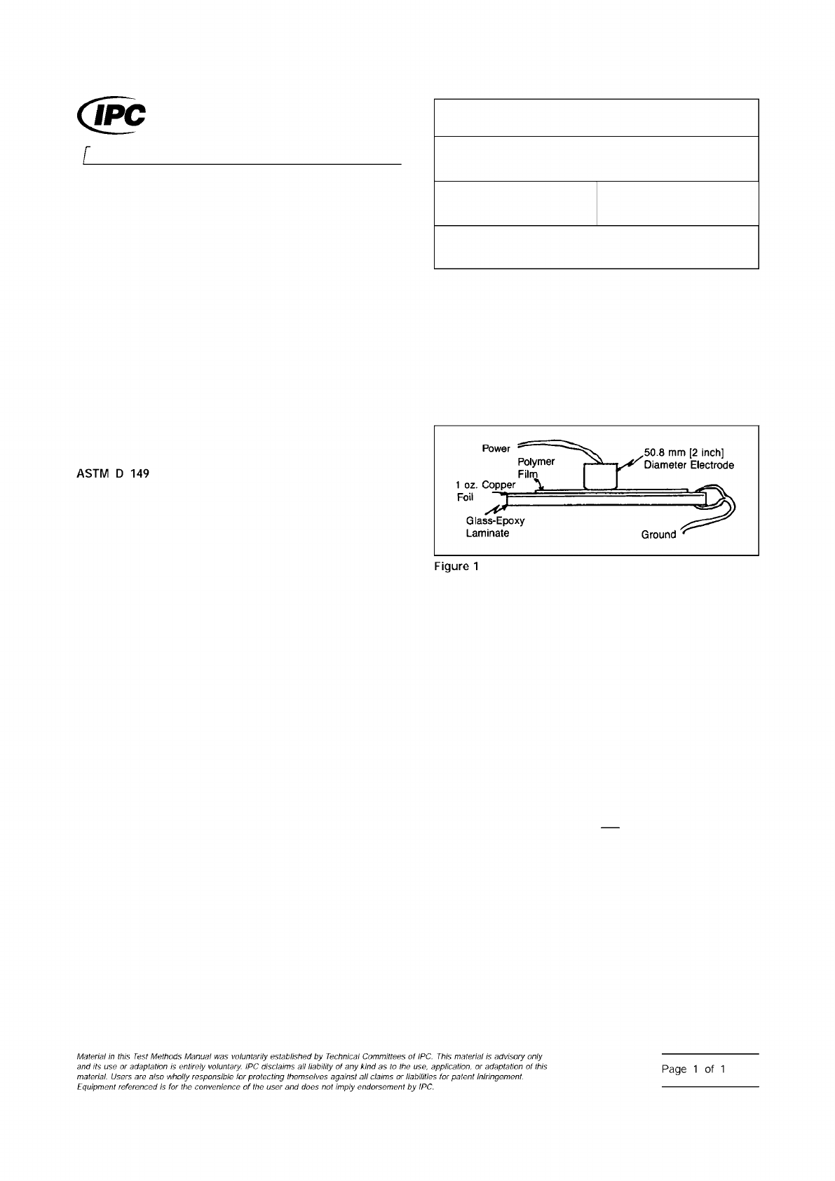
Three 102 mm x 102 mm [4.016 in x
4.016 in] squares of glass epoxy laminate materials having
1 ounce (0.0343 mm [0.00135 in] nominal) copper foil lami-
nates on one side, and having the test specimen polymer film
applied to the copper surface (see specimen preparation).
4 Apparatus
4.1
Any high voltage potential test equipment capable of
providing voltage increases of 500 VDC per second, up to at
least 10,000 VDC (see Section 6).
4.2
A standard Type 1 electrode per ASTM D 149, with a 51
mm [2.0 in] diameter, 25 mm [1.0 in] thick, with edges
rounded to 6.4 mm [0.25 in.] radius to cover the test surface.
5 Procedure
5.1 Preparation of Test Specimen
5.1.1
Cut the laminate specimen to 102 mm x 102 mm
[4.016 in x 4.016 in] and sand the edges lightly.
5.1.2
If double clad material is used, etch off all copper foil
on one side.
5.1.3
Clean the copper foil surface thoroughly, per the poly-
mer manufacturer’s recommendations, prior to applying poly-
mer coating.
5.1.4
Apply a film of the polymer test material on an area of
76.2 mm x 76.2 mm [3.0 in x 3.0 in] at the center of the cop-
per clad surface. A pinhole free film is essential.
5.1.5
Cure the polymer coating per manufacturer’s recom-
mendations.
5.2 Test
5.2.1
Clip the ground terminal of the tester over the thick-
ness of the copper foil and substrate, being careful not to let
the clip extend inward to the polymer coating (see Figure 1).
5.2.2
Place the positive electrode on top of test panel at the
center. Make certain the electrode and clip are electrically iso-
lated by the test polymer film.
5.2.3
Set up the potential voltage tester. Increase the volt-
age 500 VDC per second, until specimen exceeds require-
ment or breakdown occurs.
5.2.4
Measure the coating thickness of each of the test
specimens to the nearest 0.0025 mm [0.0001 in] in at least
four locations. Compute the average coating thickness and
standard deviation.
5.3 Evaluation
Determine the dielectric strength, E
D
, using:
E
D
=
V
BD
t
where t is the thickness of the specimen, to the nearest
0.0025 mm [0.0001 in], measured in 5.2.4 and V
BD
is
the breakdown voltage measured in 5.2.3. Record results as
‘‘V/mm’’ or ‘‘V/in.’’
6 Notes
6.1
Suggested source for tester: Hipotronics Model HD-140
from Hipotronics, Inc. Brewster, NY 10509, or equivalent.
6.2
Safety must be exercised because of the potential dan-
ger of electrical shock.
IPC-2561-1
3000 Lakeside Drive, Suite 309S
Bannockburn, IL 60015-1249
IPC-TM-650
TEST METHODS MANUAL
Number
2.5.6.1
Subject
Solder Mask - Dielectric Strength
Date
03/07
Revision
B
Originating Task Group
Solder Mask Performance Task Group (5-33b)
ASSOCIATION CONNECTING
ELECTRONICS INDUSTRIES
®
ASTM
D
149
Figure
1
Material
M
this
历
sf
Methods
Manual
was
voluntarily
established
by
Technical
Committees
of
IPC.
This
material
is
advisory
only
and
its
use
。厂
adaptation
is
entirely
voluntary.
IPC
disclaims
liability
of
any
k/nd
as
to
the
use,
application,
or
adaptation
of
this
material.
Users
are
also
wholly
responsible
for
protecting
themselves
against
claims
or
liabililies
for
patent
infringement.
Equipment
referenced
/s
for
the
convenience
of
the
user
and
does
not
imply
endorsement
by
IPC.
Page
1
of
1