IPC-TM-650 EN 2022 试验方法--.pdf - 第578页
IPC-TM-650 Page 2 of 2 Number 2.5.7 Subject Dielectric Withstanding Voltage, PCB Date 05/04 Revision D 5.2 Test (see 6.6) 5.2.1 Raise the test voltage from zero to one of the follow¬ ing specified test condition values (…
Material in this Test Methods Manual was voluntarily established by Technical Committees of IPC. This material is advisory only
and its use or adaptation is entirely voluntary. IPC disclaims all liability of any kind as to the use, application, or adaptation of this
material. Users are also wholly responsible for protecting themselves against all claims or liabilities for patent infringement.
Equipment referenced is for the convenience of the user and does not imply endorsement by IPC.
Page 1 of 2
r
ASSOCIATION
CONNECTING
/
ELECTRONICS
INDUSTRIES
®
221
5
Sanders
Road
Northbrook,
IL
60062-6135
IPC-TM-650
TEST
METHODS
MANUAL
1
Scope
The
dielectric
withstanding
voltage
test
(also
called
high-potential,
over
potential,
voltage
breakdown,
or
dielectric
strength
test)
consists
of
the
application
of
a
voltage
higher
than
rated
voltage
for
a
specific
time
between
mutually
isolated
portions
of
a
PCB
or
between
isolated
portions
and
ground.
This
is
used
to
prove
that
the
PCB
can
operate
safely
at
its
rated
voltage
and
withstand
momentary
over
potentials
due
to
switching,
surges,
and
other
similar
phenomena.
Although
this
test
is
often
called
a
voltage
breakdown
or
dielectric
strength
test,
it
is
not
intended
that
this
test
cause
insulation
breakdown
or
that
it
be
used
for
detecting
corona,
rather
it
serves
to
determine
whether
insulating
materials
and/or
conductor
spacings
are
adequate.
2
Applicable
Documents
None
3
Test
Specimen
The
test
specimen
shall
be
comprised
of
a
minimum
of
two
conductor
lines
per
conductive
layer,
suffi¬
cient
to
allow
a
voltage
to
be
applied
between
adjacent
con¬
ductor
patterns
both
between
conductive
layers
and
on
the
same
conductive
layer
(see
6.1).
4
Apparatus
or
Material
4.1
A
high
voltage
source
capable
of
supplying
the
specified
voltage
with
a
tolerance
of
土
5%
(see
6.2).
4.2
A
voltage
measuring
device
with
an
accuracy
of
5%.
If
leakage
current
measuring
capability
is
required,
the
device
shall
be
capable
of
detecting
the
leakage
current
to
within
5%
of
the
requirement.
4.3
Soft
bristle
brush
4.4
Deionized
or
distilled
water
(2
megohm-cm
minimum
resistivity
recommended)
4.5
Isopropyl
alcohol
Number
2.5.7
Subject
Dielectric
Withstanding
Voltage,
PCB
Date
Revision
05/04
D
Originating
Task
Group
Rigid
Printed
Board
Performance
Task
Group
(D-33a)
5
Procedure
5.1
Specimen
Preparation
(see
6.3)
5.1.1
Positive,
permanent,
and
noncontaminating
identifica¬
tion
of
test
specimen
is
of
paramount
importance.
5.1.2
Visually
inspect
the
test
specimens
for
any
obvious
defects,
as
described
in
the
applicable
performance
specifica¬
tion.
If
there
is
any
doubt
about
the
overall
quality
of
any
test
specimen,
the
test
specimen
should
be
replaced
and
this
replacement
noted.
5.1.3
Solder
single
stranded
(to
simulate
discrete
compo¬
nent
axial
leads)
polytetrafl
u
roet
hylene
(PTFE)
insulated
wires
in
each
of
the
connection
points
of
the
test
specimens.
These
wires
will
be
used
to
connect
the
test
patterns
of
the
test
specimens
to
the
high
voltage
source.
5.1.4
Wet
test
lead
terminals
with
deionized
or
distilled
water
and
scrub
with
a
soft
bristle
brush
for
a
minimum
of
30
seconds.
During
the
remainder
of
the
test
specimen
prepara¬
tion,
handle
test
specimens
by
the
edges
only
(see
6.4).
5.1.5
Spray
rinse
thoroughly
with
deionized
or
distilled
water.
Hold
test
specimen
at
an
approximate
30°
angle
and
spray
from
top
to
bottom.
5.1.6
Wet
test
lead
terminals
with
clean
isopropyl
alcohol
and
agitate
for
a
minimum
of
30
seconds.
Scrub
with
a
soft
bristle
brush
to
remove
flux
residue.
5.1.7
Rinse
cleaned
area
thoroughly
with
fresh
isopropyl
alcohol.
5.1.8
Dry
test
specimens
in
a
drying
oven
for
a
minimum
of
three
hours
at
an
oven
temperature
of
between
49
to
60
(120
°F
to
140
°F).
4.6
Drying
oven
5.1
.9
Allow
the
test
specimens
to
cool
to
room
temperature,
(see
6.5)
IPC-TM-650
Page 2 of 2
Number
2.5.7
Subject
Dielectric
Withstanding
Voltage,
PCB
Date
05/04
Revision
D
5.2
Test
(see
6.6)
5.2.1
Raise
the
test
voltage
from
zero
to
one
of
the
follow¬
ing
specified
test
condition
values
(see
6.2)
as
uniformly
as
possible,
at
a
rate
of
approximately
100
volts
DC
per
second.
If
the
test
condition
is
not
specified
Condition
A
shall
be
the
default.
Condition
A:
500+1
5/-0
volts
DC
Condition
B:
1
000+25/-0
volts
DC
5.2.2
Maintain
the
test
voltage
at
the
specified
value
for
a
period
of
30+3/-0
seconds.
5.2.3
Upon
completion
of
the
test,
the
test
voltage
shall
be
gradually
reduced
to
avoid
surges.
5.3
Evaluation
Examine
the
test
specimens
and
note
any
evidence
of
inadequate
insulating
materials
and/or
conductor
spacing
(i.e.,
visually
inspect
for
flashover,
sparkover
or
break¬
down
between
conductor
patterns
or
between
conductor
pat¬
terns
and
mounting
hardware).
6
Notes
6.1
Recommended
test
specimens
include
"Y''
test
pat¬
terns
(also
referred
to
as
“E”
test
coupons)
or
“comb
pat¬
terns.”
Production
printed
boards
may
also
be
used
as
test
specimens.
6.2
Performance
specifications
should
specify
the
high
volt¬
age
test
condition
and
any
deviations
to
this
test
method.
If
no
test
condition
is
specified,
use
test
condition
A.
6.3
This
test
method
may
be
performed
on
test
specimens
which
have
previously
been
prepared
and
tested
for
moisture
and
insulation
resistance.
6.4
Alternative
cleaning
procedures
may
be
implemented
if
there
is
a
concern
that
scrubbing
will
adversely
affect
test
results,
e.g.,
when
the
test
specimens
have
very
fine
spacing
and/or
are
plated
with
soft
metals
(tin/lead,
gold,
etc.).
6.5
Insulating
compound
(conformal
coating)
may
be
applied
to
the
test
specimens
following
soldering
and
clean¬
ing.
Any
coating
application
and
cure
shall
be
as
specified
by
the
coating
supplier.
6.6
The
testing
process
outlined
in
5.2
should
be
used
for
qualification
testing.
For
in-plant
quality
conformance
testing,
the
following
testing
modifications
may
be
chosen:
6.6.1
At
the
option
of
the
customer,
reduced
time
with
a
possible
correlated
higher
test
voltage
may
be
used.
6.6.2
At
the
option
of
the
customer,
an
AC
test
voltage
may
be
applied.
6.6.3
At
the
option
of
the
customer,
the
test
voltage
may
be
applied
instantaneously.
IPC-CC-830
IPC-A-600
MIL-STD-202
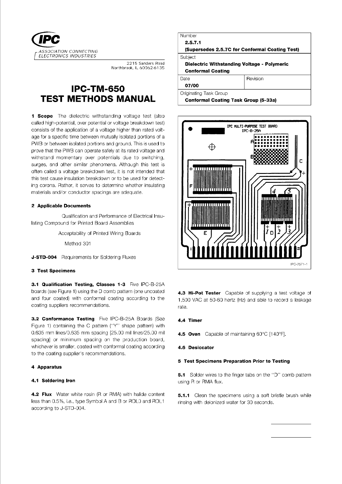
Figure 1 IPC-B-25A Test Board (Leads on D Pattern Are
Identified)
Material in this Test Methods Manual was voluntarily established by Technical Committees of IPC. This material is advisory only
and its use or adaptation is entirely voluntary. IPC disclaims all liability of any kind as to the use, application, or adaptation of this
material. Users are also wholly responsible for protecting themselves against all claims or liabilities for patent infringement.
Equipment referenced is for the convenience of the user and does not imply endorsement by IPC.
Page 1 of 2
ASSOCIATION
CONNECTING
/
ELECTRONICS
INDUSTRIES
221
5
Sanders
Road
Northbrook,
IL
60062-61
35
IPC-TM-650
TEST
METHODS
MANUAL
1
Scope
The
dielectric
withstanding
voltage
test
(also
called
high-potential,
over
potential
or
voltage
breakdown
test)
consists
of
the
application
of
a
voltage
higher
than
rated
volt¬
age
for
a
specific
time
between
mutually
isolated
portions
of
a
PWB
or
between
isolated
portions
and
ground.
This
is
used
to
prove
that
the
PWB
can
operate
safely
at
its
rated
voltage
and
withstand
momentary
over
potentials
due
to
switching,
surges,
and
other
similar
phenomena.
Although
this
test
is
often
called
a
voltage
breakdown
test,
it
is
not
intended
that
this
test
cause
insulation
breakdown
or
to
be
used
for
detect¬
ing
corona.
Rather,
it
serves
to
determine
whether
insulating
materials
and/or
conductor
spacings
are
adequate.
2
Applicable
Documents
Qualification
and
Performance
of
Electrical
Insu¬
lating
Compound
for
Printed
Board
Assemblies
Acceptability
of
Printed
Wiring
Boards
Method
301
j-STD-004
Requirements
for
Soldering
Fluxes
3
Test
Specimens
3.1
Qualification
Testing,
Classes
1-3
Five
IPC-B-25A
boards
(see
Figure
1)
using
the
D
comb
pattern
(one
un
coated
and
four
coated)
with
conformal
coating
according
to
the
coating
suppliers
recommendations.
3.2
Conformance
Testing
Five
IPC-B-25A
Boards
(See
Figure
1)
containing
the
C
pattern
("Y”
shape
pattern)
with
0.635
mm
lines/0.635
mm
spacing
[25.00
mil
lines/25.00
mil
spacing]
or
minimum
spacing
on
the
production
board,
whichever
is
smaller,
coated
with
conformal
coating
according
to
the
coating
supplier's
recommendations.
4
Apparatus
4.1
Soldering
Iron
4.2
Flux
Water
white
rosin
(R
or
RMA)
with
halide
content
less
than
0.5%,
i.e.,
type
Symbol
A
and
B
or
ROLO
and
ROL1
according
to
J-STD-004.
Number
2.5.7.1
(Supersedes
2.5.7C
for
Conformal
Coating
Test)
Subject
Dielectric
Withstanding
Voltage
-
Polymeric
Conformal
Coating
Date
Revision
07/00
Originating
Task
Group
Conformal
Coating
Task
Group
(5-33a)
IPC-2571-1
4.3
Hi-Pot
Tester
Capable
of
supplying
a
test
voltage
of
1
,500
VAC
at
50-60
hertz
(Hz)
and
able
to
record
a
leakage
rate.
4.4
Timer
4.5
Oven
Capable
of
maintaining
60℃
[140°F].
4.6
Desiccator
5
Test
Specimens
Preparation
Prior
to
Testing
5.1
Solder
wires
to
the
finger
tabs
on
the
"D”
comb
pattern
using
R
or
RMA
flux.
5.1.1
Clean
the
specimens
using
a
soft
bristle
brush
while
rinsing
with
deionized
water
for
30
seconds.