IPC-TM-650 EN 2022 试验方法--.pdf - 第580页
IPC-TM-650 Page 2 of 2 Number 2.5.7.1 Subject Dielectric Withstanding Voltage - Polymeric Conformal Coating Date 07/00 Revision 5.1.2 Immerse and agitate the test specimens in 2-propanol for 30 seconds. Scrub with a soft…
IPC-CC-830
IPC-A-600
MIL-STD-202
Figure 1 IPC-B-25A Test Board (Leads on D Pattern Are
Identified)
Material in this Test Methods Manual was voluntarily established by Technical Committees of IPC. This material is advisory only
and its use or adaptation is entirely voluntary. IPC disclaims all liability of any kind as to the use, application, or adaptation of this
material. Users are also wholly responsible for protecting themselves against all claims or liabilities for patent infringement.
Equipment referenced is for the convenience of the user and does not imply endorsement by IPC.
Page 1 of 2
ASSOCIATION
CONNECTING
/
ELECTRONICS
INDUSTRIES
221
5
Sanders
Road
Northbrook,
IL
60062-61
35
IPC-TM-650
TEST
METHODS
MANUAL
1
Scope
The
dielectric
withstanding
voltage
test
(also
called
high-potential,
over
potential
or
voltage
breakdown
test)
consists
of
the
application
of
a
voltage
higher
than
rated
volt¬
age
for
a
specific
time
between
mutually
isolated
portions
of
a
PWB
or
between
isolated
portions
and
ground.
This
is
used
to
prove
that
the
PWB
can
operate
safely
at
its
rated
voltage
and
withstand
momentary
over
potentials
due
to
switching,
surges,
and
other
similar
phenomena.
Although
this
test
is
often
called
a
voltage
breakdown
test,
it
is
not
intended
that
this
test
cause
insulation
breakdown
or
to
be
used
for
detect¬
ing
corona.
Rather,
it
serves
to
determine
whether
insulating
materials
and/or
conductor
spacings
are
adequate.
2
Applicable
Documents
Qualification
and
Performance
of
Electrical
Insu¬
lating
Compound
for
Printed
Board
Assemblies
Acceptability
of
Printed
Wiring
Boards
Method
301
j-STD-004
Requirements
for
Soldering
Fluxes
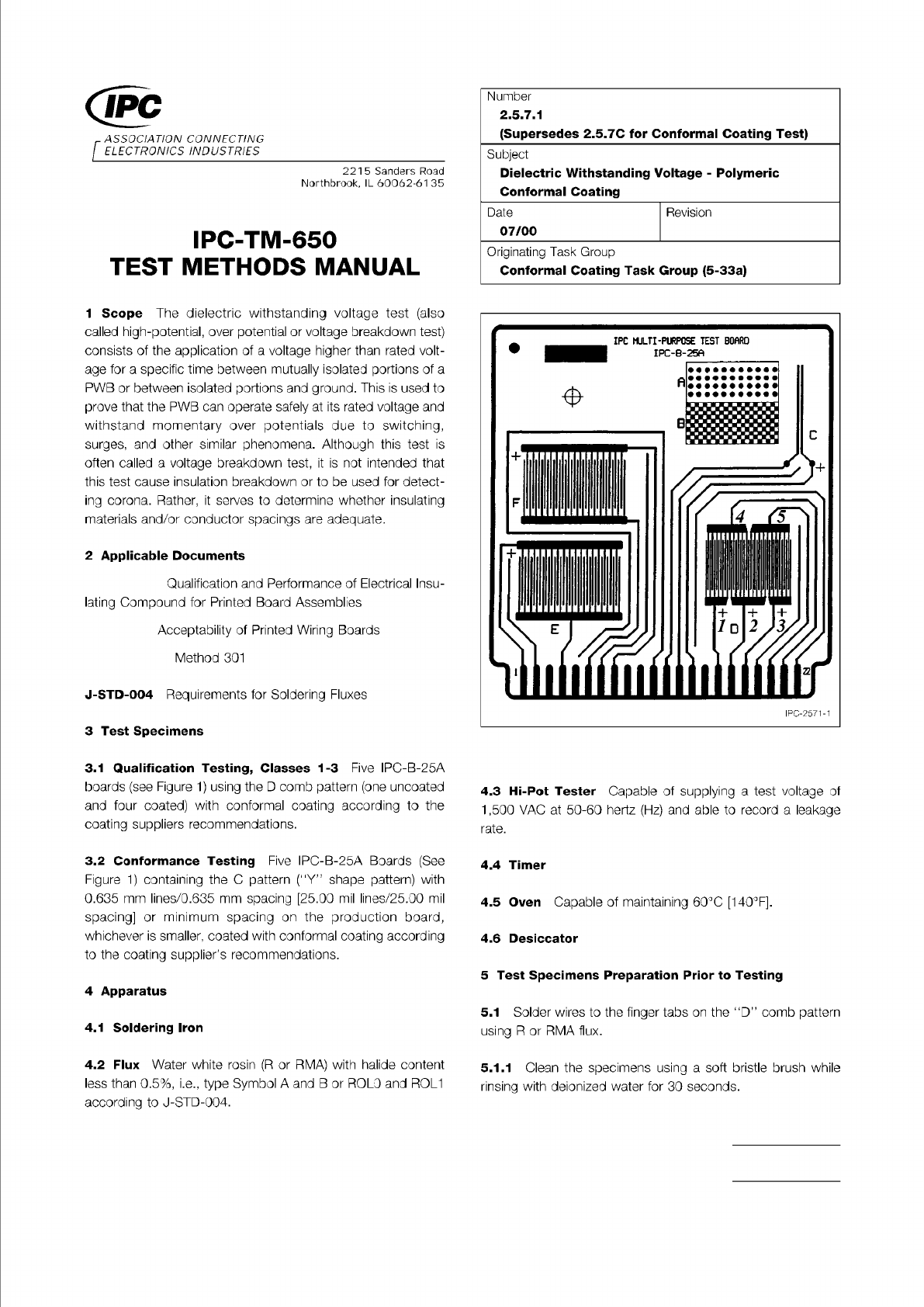
3
Test
Specimens
3.1
Qualification
Testing,
Classes
1-3
Five
IPC-B-25A
boards
(see
Figure
1)
using
the
D
comb
pattern
(one
un
coated
and
four
coated)
with
conformal
coating
according
to
the
coating
suppliers
recommendations.
3.2
Conformance
Testing
Five
IPC-B-25A
Boards
(See
Figure
1)
containing
the
C
pattern
("Y”
shape
pattern)
with
0.635
mm
lines/0.635
mm
spacing
[25.00
mil
lines/25.00
mil
spacing]
or
minimum
spacing
on
the
production
board,
whichever
is
smaller,
coated
with
conformal
coating
according
to
the
coating
supplier's
recommendations.
4
Apparatus
4.1
Soldering
Iron
4.2
Flux
Water
white
rosin
(R
or
RMA)
with
halide
content
less
than
0.5%,
i.e.,
type
Symbol
A
and
B
or
ROLO
and
ROL1
according
to
J-STD-004.
Number
2.5.7.1
(Supersedes
2.5.7C
for
Conformal
Coating
Test)
Subject
Dielectric
Withstanding
Voltage
-
Polymeric
Conformal
Coating
Date
Revision
07/00
Originating
Task
Group
Conformal
Coating
Task
Group
(5-33a)
IPC-2571-1
4.3
Hi-Pot
Tester
Capable
of
supplying
a
test
voltage
of
1
,500
VAC
at
50-60
hertz
(Hz)
and
able
to
record
a
leakage
rate.
4.4
Timer
4.5
Oven
Capable
of
maintaining
60℃
[140°F].
4.6
Desiccator
5
Test
Specimens
Preparation
Prior
to
Testing
5.1
Solder
wires
to
the
finger
tabs
on
the
"D”
comb
pattern
using
R
or
RMA
flux.
5.1.1
Clean
the
specimens
using
a
soft
bristle
brush
while
rinsing
with
deionized
water
for
30
seconds.
IPC-TM-650
Page 2 of 2
Number
2.5.7.1
Subject
Dielectric
Withstanding
Voltage
-
Polymeric
Conformal
Coating
Date
07/00
Revision
5.1.2
Immerse
and
agitate
the
test
specimens
in
2-propanol
for
30
seconds.
Scrub
with
a
soft
bristle
brush
and
spray
with
clean
2-propanol.
5.1.3
Place
the
cleaned
specimens
in
an
oven
maintained
at
50℃
[1
22°F]
for
three
to
five
hours
to
dry.
5.1.4
Remove
the
specimens
from
the
oven
and
place
in
a
desiccator
to
cool.
5.1.5
Conformal
coat
the
test
specimens
and
cure
in
accor¬
dance
with
the
suppliers
recommendations.
If
the
specimens
are
not
used
immediately,
seal
the
specimens
in
Kapac®
bags.
5.2
Procedure
5.2.1
For
each
individual
specimen,
secure
all
the
positive
leads
(1
,
3
and
5)
together
and
the
negative
(2
and
4)
together.
5.2.2
Attach
the
leads
of
the
Hi-Pot
Tester
to
the
wires
of
the
test
specimen.
5.2.3
Raise
the
test
voltage
from
zero
to
1,500
VAC
at
1
00
VAC
per
second.
5.2.4
Apply
the
test
voltage
of
1
,500
VAC
at
50-60
Hz
for
one
minute
and
record
any
leakage
rate.
5.2.5
After
the
one-minute
duration,
turn
off
the
voltage
and
disconnect
the
test
specimen
from
the
Hi-Pot
Tester.
6.0
Evaluate
6.1
Record
if
the
specimen
exhibits
flashover,
sparkover
or
breakdown.
6.1.1
Record
the
leakage
current
of
each
specimen.
1 Scope
The dielectric withstanding voltage test (Hipot test)
consists of the application of a voltage higher than the oper-
ating voltage for a specific time across the thickness of the
test specimen’s dielectric layer. This is used to prove that a
printed board can operate safely at its rated voltage and with-
stand momentary voltage spikes due to switching, surges,
and other similar phenomena. Although this test is similar to a
voltage breakdown test, it is not intended for this test to cause
insulation breakdown. Rather, it serves to determine whether
the test specimen’s layers have adequate withstanding volt-
age. This document is applicable to thin dielectric materials
such as those defined by IPC-4821.
The results can be indicative of a change or a deviation from
the normal material characteristics resulting from manufactur-
ing, processing or aging conditions. The test is useful for qual-
ity acceptance and in the determination of the suitability of the
material for a given application and may be adapted for pro-
cess control.
2 Applicable Documents
Specification for Embedded Passive Device
Capacitor Materials for Rigid and Multilayer Printed Boards
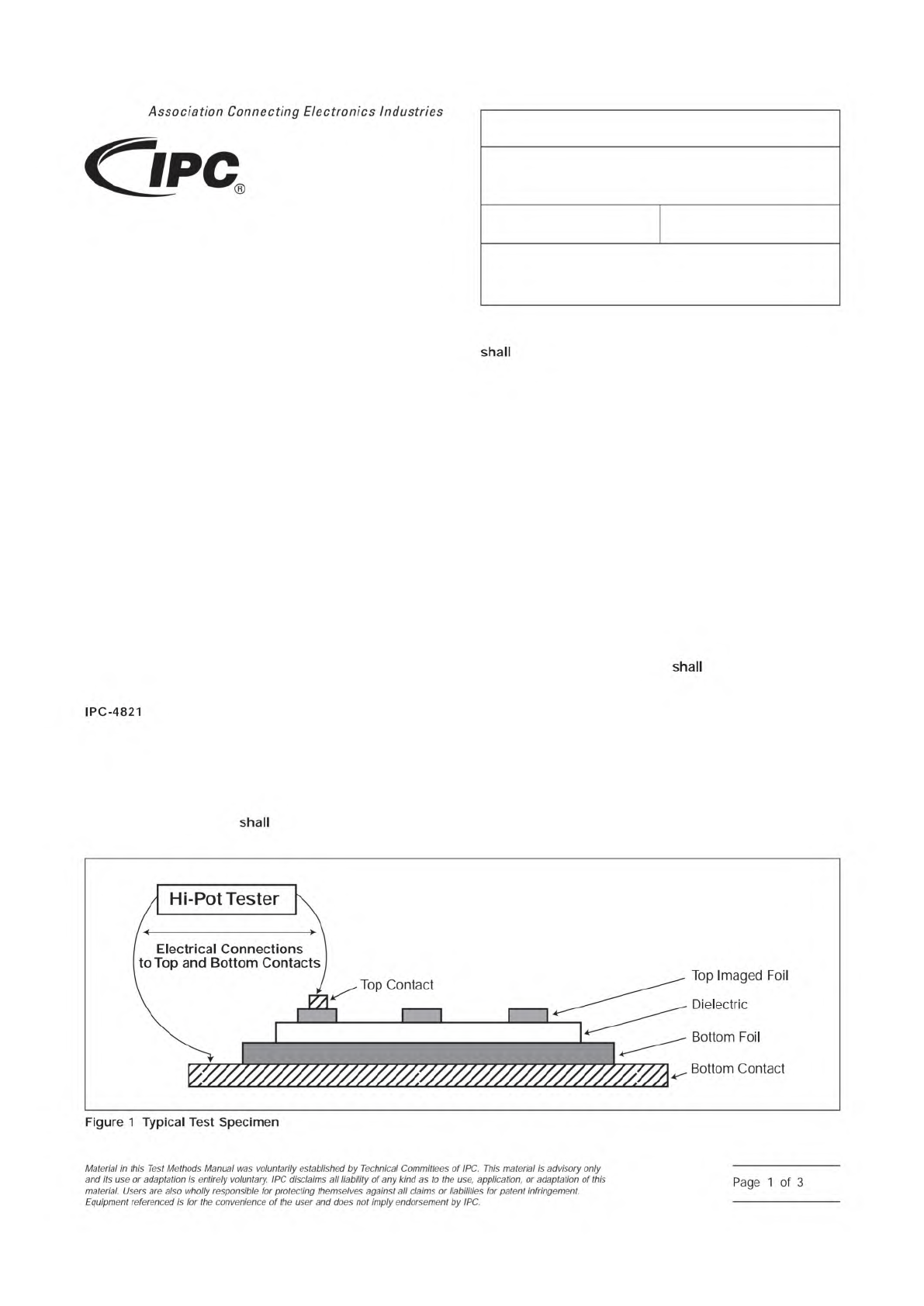
3 Test Specimen
3.1 Qualification Testing
For laminate-like capacitor
materials, test specimens
be 50 mm [1.97 in] diameter
circular electrodes (see ‘‘Top Imaged Foil’’ in Figure 1) that
be formed by imaging and then etching the copper foil,
unless otherwise as agreed upon by user and supplier
(AABUS). Spacing between adjacent Top Imaged Foil con-
ductors is recommended to be ≥100 times the dielectric thick-
ness. In order to avoid field gradient and mechanical stress
concentration, which can cause faulty dielectric breakdown,
the Bottom Foil can be either a circle larger than the Top
Imaged Foil or can be a continuous copper sheet. The con-
tinuous copper sheet will be required for very thin capacitor
dielectric layers that are not self-supporting.
For nonlaminate-like capacitor materials, the test specimen’s
Top Imaged Foil can be a size other than a 50 mm [1.97 in]
diameter circle, if this size is not practical or typical. The test
specimen’s Top Imaged Foil size for these nonlaminate-like
materials should be set to the largest size normally recom-
mended for this product (see 5.2.4). The thickness for the test
specimens should be the typical/recommended thickness. A
minimum of five test specimens
be tested for qualifica-
tion.
3.2 Conformance Testing
Test specimens can be the
same as used for qualification testing or can be other sizes or
shapes. For testing in printed board environments, actual
innerlayer power and ground features are typically used,
although other board features or test specimens can also be
used. Please note that adjustments for capacitor plate size are
required in the test procedure (see Section 6).
IPC-2572-1.eps
3000 Lakeside Drive, Suite 309S
Bannockburn, IL 60015-1249
IPC-TM-650
TEST METHODS MANUAL
Number
2.5.7.2
Subject
Dielectric Withstanding Voltage (Hipot Method) -
Thin Dielectric Layers for Printed Boards
Date
11/2009
Revision
A
Originating Task Group
Embedded Devices Test Methods Subcommittee
(D-54)
Association
Connecting
Electronics
Industries
shall
IPC-4821
shall
shall
Top
Imaged
Foil
Dielectric
Bottom
Foil
Bottom
Contact
Figure
1
Typical
Test
Specimen
Material
/n
this
Test
Methods
Manual
was
voluntarily
established
by
Technical
Committees
of
I
PC.
This
material
/s
advisory
only
and
"s
use
or
adaptation
,
s
entirely
voluntary.
IPC
disclaims
all
liability
of
any
kind
as
to
the
use,
application,
or
adaptation
of
this
material.
Users
are
also
wholly
responsible
for
protecting
themselves
against
all
claims
or
liabilities
for
patent
infringement.
Equipment
referenced
/s
for
the
convenience
of
the
user
and
does
not
imply
endorsement
by
IPC.
Page
1
of
3