IPC-TM-650 EN 2022 试验方法--.pdf - 第584页
Figure 1 Suggested Flex Circuit La yout for Insulation Resistance T est Figure 2 Pr eattachment of the ACF Strips t o the Flex Circuit The Institute for Int erconnecting and Packaging E lectronic Circuits 2215 Sanders Ro…

current preset on the Hipot test instrument, causing the
instrument to indicate a failure when in fact there was none.
The charging current of the capacitor is affected by the
change in voltage from one ramp step to another, the dielec-
tric constant of the dielectric, the thickness of the dielectric
and the area of the capacitor. High dielectric constant, very
thin dielectric thickness and large area of the capacitor plates
will all cause the charging current to increase. As a result, the
threshold current setting on the Hipot test instrument may
need to be adjusted to avoid generating a false failure condi-
tion.
6.2
Some thin and filled dielectrics will require a higher
threshold current setting, compared to unfilled materials. This
is particularly true of dielectrics containing ferroelectric com-
pounds, such as barium titanate. These materials may show
a nonlinear response between current and voltage. This is not
an issue at most operating voltages, which are normally low,
but can be an issue for the Hipot test. At high voltage levels,
these materials may trigger a false failure because they allow
more current than the threshold setting.
6.3
Materials, especially very thin and/or highly filled materi-
als, may have a leakage current per unit area that is area
dependent when tested at the specified test voltage. Thus,
results from the qualification test specimen or other small area
test structures may not reflect the actual leakage current per
unit area when the material is tested in a significantly larger
area format, such as that commonly done in conformance
testing by a material supplier.
6.4 Reference Documents
‘‘Dielectric Breakdown Voltage of Solid Electri-
cal Insulating Materials at Commercial Power Frequencies’’
Number
2.5.7.2
Subject
Dielectric Withstanding Voltage (Hipot Method) - Thin Dielectric
Layers for Printed Boards
Date
11/2009
Revision
A
IPC-TM-650
ASTM
D149
Page
3
of
3
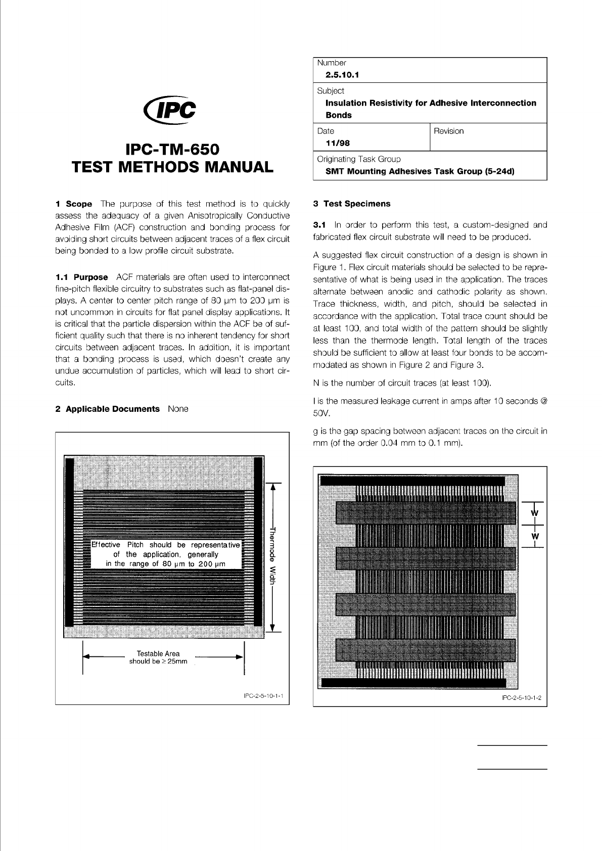
Figure 1 Suggested Flex Circuit Layout for Insulation
Resistance Test
Figure 2 Preattachment of the ACF Strips to the Flex
Circuit
The Institute for Interconnecting and Packaging Electronic Circuits
2215 Sanders Road • Northbrook, IL 60062
Material in this Test Methods Manual was voluntarily established by Technical Committees of the IPC. This material is advisory only
and its use or adaptation is entirely voluntary. IPC disclaims all liability of any kind as to the use, application, or adaptation of this
material. Users are also wholly responsible for protecting themselves against all claims or liabilities for patent infringement.
Equipment referenced is for the convenience of the user and does not imply endorsement by the IPC.
Page 1 of 2
Number
Testable
Area
should
be
25mm
IPC-TM-650
TEST
METHODS
MANUAL
1
Scope
The
purpose
of
this
test
method
is
to
quickly
assess
the
adequacy
of
a
given
Anisotropically
Conductive
Adhesive
Film
(ACF)
construction
and
bonding
process
for
avoiding
short
circuits
between
adjacent
traces
of
a
flex
circuit
being
bonded
to
a
low
profile
circuit
substrate.
1.1
Purpose
ACF
materials
are
often
used
to
interconnect
fine-pitch
flexible
circuitry
to
substrates
such
as
flat-panel
dis¬
plays.
A
center
to
center
pitch
range
of
80
pm
to
200
pm
is
not
uncommon
in
circuits
for
flat
panel
display
applications.
It
is
critical
that
the
particle
dispersion
within
the
ACF
be
of
suf¬
ficient
quality
such
that
there
is
no
inherent
tendency
for
short
circuits
between
adjacent
traces.
In
addition,
it
is
important
that
a
bonding
process
is
used,
which
doesn't
create
any
undue
accumulation
of
particles,
which
will
lead
to
short
cir¬
cuits.
2
Applicable
Documents
None
2.5.10.1
Subject
Insulation
Resistivity
for
Adhesive
Interconnection
Bonds
Date
Revision
11/98
Originating
Task
Group
SMT
Mounting
Adhesives
Task
Group
(5-24d)
3
Test
Specimens
3.1
In
order
to
perform
this
test,
a
custom-designed
and
fabricated
flex
circuit
substrate
will
need
to
be
produced.
A
suggested
flex
circuit
construction
of
a
design
is
shown
in
Figure
1
.
Flex
circuit
materials
should
be
selected
to
be
repre¬
sentative
of
what
is
being
used
in
the
application.
The
traces
alternate
between
anodic
and
cathodic
polarity
as
shown.
Trace
thickness,
width,
and
pitch,
should
be
selected
in
accordance
with
the
application.
Total
trace
count
should
be
at
least
1
00,
and
total
width
of
the
pattern
should
be
slightly
less
than
the
thermode
length.
Total
length
of
the
traces
should
be
sufficient
to
allow
at
least
four
bonds
to
be
accom¬
modated
as
shown
in
Figure
2
and
Figure
3.
N
is
the
number
of
circuit
traces
(at
least
100).
I
is
the
measured
leakage
current
in
amps
after
10
seconds
@
50V.
g
is
the
gap
spacing
between
adjacent
traces
on
the
circuit
in
mm
(of
the
order
0.04
mm
to
0.1
mm).
wi
a
h
IPC-2-5-1
0-1-1
IPC-2-5-10-1-2
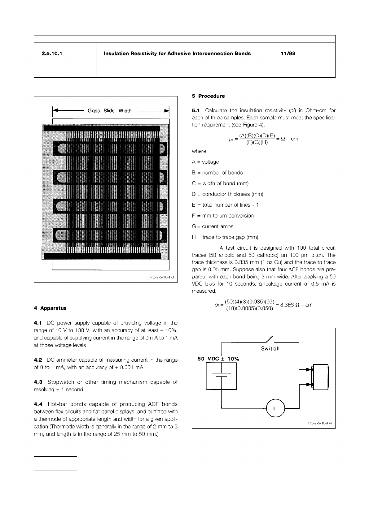
Example
Figure 3 Flex Circuit Containing Four ACF Bond Sites,
After Being Bonded to a Glass Slide
Figure 4 Schematic Diagram for Insulation Resistivity
Measurement
IPC-TM-650
Number
Subject Date
Revision
Page 2 of 2
2.5.10.1
Insulation
Resistivity
for
Adhesive
Interconnection
Bonds
11/98
4
Apparatus
4.1
DC
power
supply
capable
of
providing
voltage
in
the
range
of
1
0
V
to
100
V,
with
an
accuracy
of
at
least
±
10%,
and
capable
of
supplying
current
in
the
range
of
0
mA
to
1
mA
at
those
voltage
levels
4.2
DC
ammeter
capable
of
measuring
current
in
the
range
of
0
to
1
mA,
with
an
accuracy
of
土
0.001
mA
4.3
Stopwatch
or
other
timing
mechanism
capable
of
resolving
±
1
second
4.4
Hot-bar
bonds
capable
of
producing
ACF
bonds
between
flex
circuits
and
flat
panel
displays,
and
outfitted
with
a
thermode
of
appropriate
length
and
width
for
a
given
appli¬
cation
(Thermode
width
is
generally
in
the
range
of
2
mm
to
3
mm,
and
length
is
in
the
range
of
25
mm
to
50
mm.)
5
Procedure
5.1
Calculate
the
insulation
resistivity
(pi)
in
Ohm-cm
for
each
of
three
samples.
Each
sample
must
meet
the
specifica¬
tion
requirement
(see
Figure
4).
where:
(A)(B)(C)(D)(E)
(F)(G)(H)
=
Q
-
cm
A
二
voltage
B
二
number
of
bonds
C
=
width
of
bond
(mm)
D
=
conductor
thickness
(mm)
E
=
total
number
of
lines
-
1
F
=
mm
to
pm
conversion
G
二
current
amps
H
=
trace
to
trace
gap
(mm)
A
test
circuit
is
designed
with
100
total
circuit
traces
(50
anodic
and
50
cathodic)
on
100
pm
pitch.
The
trace
thickness
is
0.035
mm
(1
oz
Cu)
and
the
trace
to
trace
gap
is
0.05
mm.
Suppose
also
that
four
ACF
bonds
are
pre¬
pared,
with
each
bond
being
3
mm
wide.
After
applying
a
50
VDC
bias
for
10
seconds,
a
leakage
current
of
0.5
mA
is
measured.
pi
=
(50)(4)(3)(0.035)(99)
(10)(0.0005)(0.050)
=
8.3E6
Q
-
cm
50
VDC
±
10%
IPC-2-5-10-1-4