IPC-TM-650 EN 2022 试验方法--.pdf - 第617页
45° angle results in a square 1.08 mm x 1.08 mm [0.04252 in x 0.04252 in] grid. Note: the sketches do not look square when tipped 45° but, the CAF Test Boards do. The resulting via ed ge to vi a e dge sp acin gs ar e: 0 …
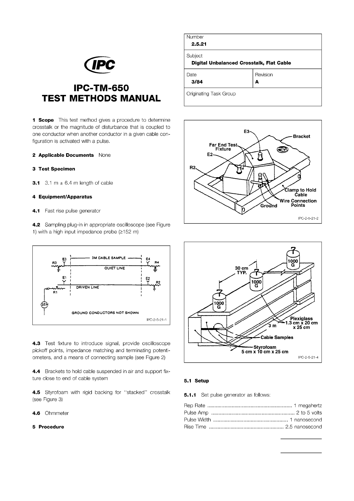
Figure 1 Oscilloscope
Figure 2 Connecting Sample
Figure 3 Crosstalk
The Institute for Interconnecting and Packaging Electronic Circuits
2215 Sanders Road • Northbrook, IL 60062
Material in this Test Methods Manual was voluntarily established by Technical Committees of the IPC. This material is advisory only
and its use or adaptation is entirely voluntary. IPC disclaims all liability of any kind as to the use, application, or adaptation of this
material. Users are also wholly responsible for protecting themselves against all claims or liabilities for patent infringement.
Equipment referenced is for the convenience of the user and does not imply endorsement by the IPC.
Page 1 of 2
回
IPC-TM-650
TEST
METHODS
MANUAL
1
Scope
This
test
method
gives
a
procedure
to
determine
crosstalk
or
the
magnitude
of
disturbance
that
is
coupled
to
one
conductor
when
another
conductor
in
a
given
cable
con¬
figuration
is
activated
with
a
pulse.
2
Applicable
Documents
None
3
Test
Specimen
3.1
3.1
m
±
6.4
m
length
of
cable
4
Equipment/Apparatus
4.1
Fast
rise
pulse
generator
4.2
Sampling
plug-in
in
appropriate
oscilloscope
(see
Figure
1)
with
a
high
input
impedance
probe
Q152
m)
GROUND
CONDUCTORS
NOT
SHOWN
I
PC-2-5-21-1
4.3
Test
fixture
to
introduce
signal,
provide
oscilloscope
pickoff
points,
impedance
matching
and
terminating
potenti¬
ometers,
and
a
means
of
connecting
sample
(see
Figure
2)
4.4
Brackets
to
hold
cable
suspended
in
air
and
support
fix¬
ture
close
to
end
of
cable
system
4.5
Styrofoam
with
rigid
backing
for
"stacked”
crosstalk
(see
Figure
3)
4.6
Ohmmeter
5
Procedure
Number
2.5.21
Subject
Digital
Unbalanced
Crosstalk,
Flat
Cable
Date
3/84
Revision
A
Originating
Task
Group
5.1
Setup
5.1.1
Set
pulse
generator
as
follows:
.....
1
megahertz
2
to
5
volts
..
1
nanosecond
2.5
nanosecond
Rep
Rate
...
Pulse
Amp
Pulse
Width
Rise
Time
..
45° angle results in a square 1.08 mm x 1.08 mm [0.04252 in
x 0.04252 in] grid. Note: the sketches do not look square
when tipped 45° but, the CAF Test Boards do. The resulting
via edge to via edge spacings are: 0.26 mm, 0.37 mm,
0.51 mm, 0.62 mm [0.0102 in, 0.0146 in, 0.0201 in,
0.0244 in]. Other than the use of different drilled hole sizes
and a small change in pad sizes, the four structures are iden-
tical. The vias in the ‘‘B’’ test structure are not aligned with the
glass fibers. If the failure mode is along glass bundles it is rea-
sonable to expect the ‘‘B’’ test structure to perform better
than the ‘‘A’’ structure for equivalent via edge to via edge
spacings. Within a given test structure, the inner and outer
layer pads for all 10 layers are the same, i.e., the same pad
size is consistently used within a given test structure although,
it does change from structure to structure. All via to electrode
connections are made on layer 1 and are repeated on layer 10
so that a single etch-out will not affect results.
A conceptual representation of the ‘‘B’’ test structure of
the coupons in Figure 1 is shown to the upper right.
Design details on each of the four ‘‘B’’ test structures follows
in Table 2.
3.2 Other Structures
Section C is designed to evaluate
plated-through hole (PTH)-to-plane layer spacings. It is rec-
ommended to use the registration coupon per test board (IPC
Test Pattern F) when CAF testing includes this region. Section
D in the IPC-9254 design is for layer-to-layer Z-axis CAF test-
ing. Section D in the IPC-9253 is for evaluating CAF resis-
tance in a press-fit compliant pin connector application. The
feature in the D region is an optional feature that is present
automatically with the design. However, the A, B and C
regions
remain as designed in order to provide a stan-
dard basis of comparison.
The CAF test board with 10 layers is designated to evaluate
thin single-ply constructions typically used on high perfor-
mance boards. This board construction stackup can be
reduced down to: (a) four layers by eliminating layers 3
through 8 and (b) only test structures A and B, when just
evaluating differences between laminate materials.
3.3 CAF Test Board Design
This 10-layer CAF test board
for evaluating the insulation resistance between internal con-
ductors within a printed wiring board has the following key
features for evaluating hole-hole CAF resistance (Figure 3).
Holes In-Line (in-line with glass fiber direction): There are two
rows of 42 signal-1 vias intermeshed with three rows of 42
Outer layer pad size 0.86 mm [0.0339 in] 0.81 mm [0.0319 in] 0.75 mm [0.0295 in] 0.69 mm [0.0272 in]
Inner layer pad size 0.86 mm [0.0339 in] 0.81 mm [0.0319 in] 0.75 mm [0.0295 in] 0.69 mm [0.0272 in]
Drilled hole size 0.74 mm [0.0291 in] 0.63 mm [0.0248 in] 0.51 mm [0.0201 in] 0.37 mm [0.0146 in]
Via edge to via edge
(shortest distance)
0.27 mm [0.0106 in] 0.38 mm [0.0150 in] 0.51 mm [0.0201 in] 0.65 mm [0.0256 in]
Via edge to via edge
(Manhattan Distance)
0.27 mm [0.0106 in] 0.38 mm [0.0150 in] 0.51 mm [0.0201 in] 0.65 mm [0.0256 in]
On IPC-9254
, bias
applied between:
J1, J5 J2, J5 J3, J5 J4, J5
IPC-2625-2
Number
2.6.25
Subject
Conductive Anodic Filament (CAF) Resistance Test: X-Y Axis
Date
02/21
Revision
C
IPC-TM-650
—
Table
1
Test
Structures
A1
through
A4
Design
Rules
A1
A2
A3
A4
only
"Manhattan
Distance"
=
a+b
Figure
2
Manhattan
Distance
(Shortest
Orthogonal)
shall
Page
3
of
11
MIL-STD-202
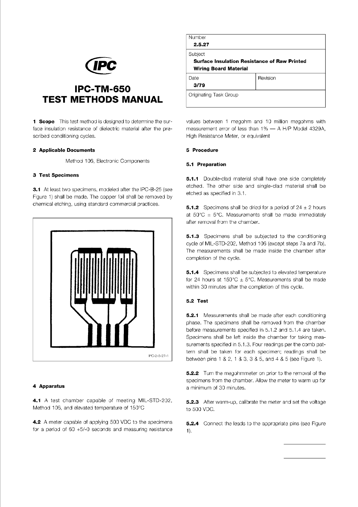
Figure 1 Surface Insulation Resistance Test Pattern
(Modeled after IPC-B25 Test Board)
The Institute for Interconnecting and Packaging Electronic Circuits
2215 Sanders Road • Northbrook, IL 60062
Material in this Test Methods Manual was voluntarily established by Technical Committees of the IPC. This material is advisory only
and its use or adaptation is entirely voluntary. IPC disclaims all liability of any kind as to the use, application, or adaptation of this
material. Users are also wholly responsible for protecting themselves against all claims or liabilities for patent infringement.
Equipment referenced is for the convenience of the user and does not imply endorsement by the IPC.
Page 1 of 2
回
IPC-TM-650
TEST
METHODS
MANUAL
1
Scope
This
test
method
is
designed
to
determine
the
sur¬
face
insulation
resistance
of
dielectric
material
after
the
pre¬
scribed
conditioning
cycles.
2
Applicable
Documents
Method
106,
Electronic
Components
3
Test
Specimens
3.1
At
least
two
specimens,
modeled
after
the
IPC-B-25
(see
Figure
1)
shall
be
made.
The
copper
foil
shall
be
removed
by
chemical
etching,
using
standard
commercial
practices.
I
PC-2-5-27-1
4
Apparatus
4.1
A
test
chamber
capable
of
meeting
MIL-STD-202,
Method
1
06,
and
elevated
temperature
of
1
50℃
4.2
A
meter
capable
of
applying
500
VDC
to
the
specimens
for
a
period
of
60
+5/-0
seconds
and
measuring
resistance
Number
2.5.27
Subject
Surface
Insulation
Resistance
of
Raw
Printed
Wiring
Board
Material
Date
Revision
3/79
Originating
Task
Group
values
between
1
megohm
and
10
million
megohms
with
measurement
error
of
less
than
1%
—
A
H/P
Model
4329A,
High
Resistance
Meter,
or
equivalent
5
Procedure
5.1
Preparation
5.1.1
Double-clad
material
shall
have
one
side
completely
etched.
The
other
side
and
single-clad
material
shall
be
etched
as
specified
in
3.1
.
5.1.2
Specimens
shall
be
dried
for
a
period
of
24
±
2
hours
at
50℃
土
5
℃.
Measurements
shall
be
made
immediately
after
removal
from
the
chamber.
5.1.3
Specimens
shall
be
subjected
to
the
conditioning
cycle
of
MIL-STD-202,
Method
106
(except
steps
7a
and
7b).
The
measurements
shall
be
made
inside
the
chamber
after
completion
of
the
cycle.
5.1.4
Specimens
shall
be
subjected
to
elevated
temperature
for
24
hours
at
150℃
±
5
℃.
Measurements
shall
be
made
within
30
minutes
after
the
completion
of
this
cycle.
5.2
Test
5.2.1
Measurements
shall
be
made
after
each
conditioning
phase.
The
specimens
shall
be
removed
from
the
chamber
before
measurements
specified
in
5.1.2
and
5.1
.4
are
taken.
Specimens
shall
be
left
inside
the
chamber
for
taking
mea¬
surements
specified
in
5.1.3.
Four
readings
per
the
comb
pat¬
tern
shall
be
taken
for
each
specimen;
readings
shall
be
between
pins
1
&
2,
1
&
3,
3
&
5,
and
4
&
5
(see
Figure
1).
5.2.2
Turn
the
megohmmeter
on
prior
to
the
removal
of
the
specimens
from
the
chamber.
Allow
the
meter
to
warm
up
for
a
minimum
of
30
minutes.
5.2.3
After
warm-up,
calibrate
the
meter
and
set
the
voltage
to
500
VDC.
5.2.4
Connect
the
leads
to
the
appropriate
pins
(see
Figure
1).