IPC-TM-650 EN 2022 试验方法--.pdf - 第619页
IPC-TM-650 Number Subject Date Revision Page 2 of 2 2.5.27 Surface Insulation Resistance of Raw Printed Wiring Board Material 3/79 5.2.5 After allowing the meter to "charge” for 60 seconds, switch to "measure” …
MIL-STD-202
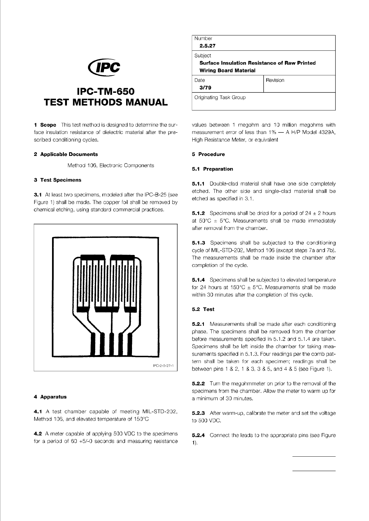
Figure 1 Surface Insulation Resistance Test Pattern
(Modeled after IPC-B25 Test Board)
The Institute for Interconnecting and Packaging Electronic Circuits
2215 Sanders Road • Northbrook, IL 60062
Material in this Test Methods Manual was voluntarily established by Technical Committees of the IPC. This material is advisory only
and its use or adaptation is entirely voluntary. IPC disclaims all liability of any kind as to the use, application, or adaptation of this
material. Users are also wholly responsible for protecting themselves against all claims or liabilities for patent infringement.
Equipment referenced is for the convenience of the user and does not imply endorsement by the IPC.
Page 1 of 2
回
IPC-TM-650
TEST
METHODS
MANUAL
1
Scope
This
test
method
is
designed
to
determine
the
sur¬
face
insulation
resistance
of
dielectric
material
after
the
pre¬
scribed
conditioning
cycles.
2
Applicable
Documents
Method
106,
Electronic
Components
3
Test
Specimens
3.1
At
least
two
specimens,
modeled
after
the
IPC-B-25
(see
Figure
1)
shall
be
made.
The
copper
foil
shall
be
removed
by
chemical
etching,
using
standard
commercial
practices.
I
PC-2-5-27-1
4
Apparatus
4.1
A
test
chamber
capable
of
meeting
MIL-STD-202,
Method
1
06,
and
elevated
temperature
of
1
50℃
4.2
A
meter
capable
of
applying
500
VDC
to
the
specimens
for
a
period
of
60
+5/-0
seconds
and
measuring
resistance
Number
2.5.27
Subject
Surface
Insulation
Resistance
of
Raw
Printed
Wiring
Board
Material
Date
Revision
3/79
Originating
Task
Group
values
between
1
megohm
and
10
million
megohms
with
measurement
error
of
less
than
1%
—
A
H/P
Model
4329A,
High
Resistance
Meter,
or
equivalent
5
Procedure
5.1
Preparation
5.1.1
Double-clad
material
shall
have
one
side
completely
etched.
The
other
side
and
single-clad
material
shall
be
etched
as
specified
in
3.1
.
5.1.2
Specimens
shall
be
dried
for
a
period
of
24
±
2
hours
at
50℃
土
5
℃.
Measurements
shall
be
made
immediately
after
removal
from
the
chamber.
5.1.3
Specimens
shall
be
subjected
to
the
conditioning
cycle
of
MIL-STD-202,
Method
106
(except
steps
7a
and
7b).
The
measurements
shall
be
made
inside
the
chamber
after
completion
of
the
cycle.
5.1.4
Specimens
shall
be
subjected
to
elevated
temperature
for
24
hours
at
150℃
±
5
℃.
Measurements
shall
be
made
within
30
minutes
after
the
completion
of
this
cycle.
5.2
Test
5.2.1
Measurements
shall
be
made
after
each
conditioning
phase.
The
specimens
shall
be
removed
from
the
chamber
before
measurements
specified
in
5.1.2
and
5.1
.4
are
taken.
Specimens
shall
be
left
inside
the
chamber
for
taking
mea¬
surements
specified
in
5.1.3.
Four
readings
per
the
comb
pat¬
tern
shall
be
taken
for
each
specimen;
readings
shall
be
between
pins
1
&
2,
1
&
3,
3
&
5,
and
4
&
5
(see
Figure
1).
5.2.2
Turn
the
megohmmeter
on
prior
to
the
removal
of
the
specimens
from
the
chamber.
Allow
the
meter
to
warm
up
for
a
minimum
of
30
minutes.
5.2.3
After
warm-up,
calibrate
the
meter
and
set
the
voltage
to
500
VDC.
5.2.4
Connect
the
leads
to
the
appropriate
pins
(see
Figure
1).
IPC-TM-650
Number
Subject Date
Revision
Page 2 of 2
2.5.27
Surface
Insulation
Resistance
of
Raw
Printed
Wiring
Board
Material
3/79
5.2.5
After
allowing
the
meter
to
"charge”
for
60
seconds,
switch
to
"measure”
and
read
the
meter
in
megohms
after
the
indicator
settles
down
(usually
within
60
seconds).
5.3
Evaluation
Readings
shall
be
recorded
to
two
signifi¬
cant
digits
in
megohms.
6
Notes
6.1
This
method
can
be
used
in
substitution
for
surface
resistance.
Volume
resistivity
cannot
be
replaced
by
this
method,
but
other
tests
such
as
dielectric
strength,
dissipa¬
tion
factor,
and
dielectric
constant
will
give
a
better
indication
of
the
electrical
properties
than
volume
resistivity.
Unbal/Bal Freq. Range Model No.
50/50 100 KHz to 125 MHz 0001 BB
50/75 100 KHz to 125 MHz 0101 BB
50/90 100 KHz to 125 MHz 0200 BB
50/100 100 KHz to 100 MHz 0300 BB
50/150 100 KHz to 100 MHz 0400 BB
The Institute for Interconnecting and Packaging Electronic Circuits
2215 Sanders Road • Northbrook, IL 60062
Material in this Test Methods Manual was voluntarily established by Technical Committees of the IPC. This material is advisory only
and its use or adaptation is entirely voluntary. IPC disclaims all liability of any kind as to the use, application, or adaptation of this
material. Users are also wholly responsible for protecting themselves against all claims or liabilities for patent infringement.
Equipment referenced is for the convenience of the user and does not imply endorsement by the IPC.
Page 1 of 4
IPC-TM-650
TEST
METHODS
MANUAL
1
Scope
This
method
is
used
to
determine
the
attenuation
of
balanced
and
unbalanced
cables.
2
Applicable
Documents
None
3
Test
Specimen
3.1
30.5
meters
of
completed
flat
cable
4
Apparatus
4.1
H.R.
Model
#8568A
or
equivalent
spectrum
analyzer
4.2
H.R.
Model
#8444A
or
equivalent
2
tracking
generator
4.3
Two
RG-223/U
or
equivalent
50
Ohm
coaxial
cables
4.4
North
Hills
or
equivalent
matching
transformers
4.5
Resistor
matching
network
(see
Figure
1)
5
Procedure
5.1
Procedure
(Balanced)
Number
2.5.30
Subject
Balanced
and
Unbalanced
Cable
Attenuation
Measurements
Date
Revision
12/87
Originating
Task
Group
5.1.2
Select
impedance
matching
transformers
that
match
(as
close
as
possible)
the
characteristic
impedance
of
the
cable
under
test.
5.1
.3
Connect
the
outputs
of
the
two
matching
transformers
together.
Sweep
the
spectrum
analyzer
through
the
required
frequency
range
to
determine
the
loss
in
the
matching
trans¬
formers.
5.1.4
Separate
the
two
matching
transformers
and
connect
30.5
m
of
the
test
cable
between
them;
again
sweep
the
spectrum
analyzer
through
the
required
frequency
range.
This
measurement
determines
the
total
loss,
which
includes
the
cable
and
matching
transformers.
5.1.5
To
determine
the
cable
attenuation,
based
on
30.5
meters
of
cable,
at
each
frequency
of
interest,
subtract
the
results
of
5.1
.3
from
the
results
of
5.1.4
(see
Figure
2).
5.2
Procedure
(Unbalanced)
5.2.1
Calculate
the
resistance
required
to
match
the
50
ohm
system
impedance
to
the
test
cable's
characteristic
imped¬
ance,
as
shown
in
Figure
1
.
5.2.2
Use
the
above
resistive
matching
network
in
place
of
the
balanced
transformers
as
indicated
in
5.1
.3.
Perform
the
unbalanced
attenuation
test
as
described
in
5.1
.1
through
5.1
.5
(see
Figure
3).
5.1.1
Calibrate
spectrum
analyzer
and
adjust
the
tracking
generator
for
accurate
frequency
tracking.