IPC-TM-650 EN 2022 试验方法--.pdf - 第624页
ANSI/J-STD-001 IPC-TM-650 The Institute for Int erconnecting and Packaging E lectronic Circuits 2215 Sanders Road • Northbrook, IL 60062 Material in this T est M ethods Manual was voluntarily establis hed by T echni cal …
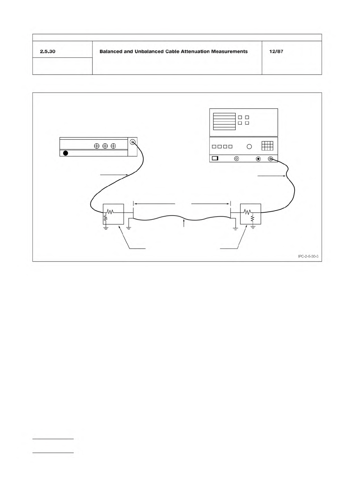
Figure 3 Unbalanced Attenuation Equipment Setup
Tracking Generator
Spectrum Analyzer
Coaxial Cable
Coaxial Cable
R
1
R
2
R
1
R
2
31 m
Cable
Resistor Matching Networks
IPC-TM-650
Number
Subject Date
Revision
Page 4 of 4
Balanced
and
Unbalanced
Cable
Attenuation
Measurements
12/87
I
PC-2-5-30-3
ANSI/J-STD-001
IPC-TM-650
The Institute for Interconnecting and Packaging Electronic Circuits
2215 Sanders Road • Northbrook, IL 60062
Material in this Test Methods Manual was voluntarily established by Technical Committees of the IPC. This material is advisory only
and its use or adaptation is entirely voluntary. IPC disclaims all liability of any kind as to the use, application, or adaptation of this
material. Users are also wholly responsible for protecting themselves against all claims or liabilities for patent infringement.
Equipment referenced is for the convenience of the user and does not imply endorsement by the IPC.
Page 1 of 5
IPC-TM-650
TEST
METHODS
MANUAL
1
Scope
EOS
and
electrostatic
discharge
(ESD)
have
been
proven
to
damage
and
degrade
electronic
components
and
assemblies.
This
test
method
consists
of
a
series
of
individual
test
procedures
to
test
soldering
and
desoldering
hand
tools
with
grounded
working
surfaces
for
electrical
grounds,
tran¬
sient
voltages,
and
current
leakage.
This
series
of
test
methods
attempts
to
identify
those
bench-
top
systems,
which
might
contribute
to
premature
assembly
failure
from
EOS/ESD
related
failure
mechanisms.
Test
results
may
be
erroneous
or
skewed
if
they
are
incorrectly
performed,
influenced
by
outside
forces
(e.g.,
air
conditioning
discharge
over
the
unit
under
test),
or
if
incorrect
test
equipment
is
selected.
Test
equipment
selected
for
equipment
qualification
must
be
capable
of
measuring
the
low
voltages
and
current
emitted
by
the
unit
under
test
(UUT).
Additionally,
the
equipment
must
be
capable
of
reading
pulses
and
frequencies
emitted
by
the
UUT,
which
may
be
oscillator
or
microprocessor
controlled.
As
faster
and
more
capable
oscillator
and
microprocessor
controlled
equipment
is
introduced
by
equipment
manufactur¬
ers,
it
may
become
necessary
to
select
test
equipment
with
a
broader
bandwidth
than
that
currently
specified
in
this
proce¬
dure.
Failure
to
do
so
is
likely
to
qualify
equipment
that
might
otherwise
be
disqualified.
Several
of
these
tests
can
be
falsely
influenced
by
radio
fre¬
quency
interference
and
electromagnetic
interference
from
lighting
and
equipment
found
in
the
workplace
and
testing
area.
To
avoid
these
influences
the
leakage
and
transient
tests
should
be
performed
in
a
screen
room.
In
lieu
of
a
screen
room,
a
separate
test
procedure
(see
Test
Method
2.5.33.4)
has
been
provided
to
make
a
low
cost
shielded
enclosure
which
should
provide
adequate
shielding
for
the
performance
of
these
test
procedures.
Warning:
These
are
laboratory
test
procedures
that
may
of
necessity
expose
terminals
that
carry
line
voltages.
All
stan¬
dard
laboratory
safety
procedures
regarding
the
setup
and
performance
of
tests
with
line
voltage
equipment
must
be
observed
at
all
times.
Caution:
These
tests
are
performed
with
soldering
systems
at
their
normal
operating
temperature.
Test
personnel
must
take
adequate
precautionary
steps
to
protect
themselves
and
others
from
potential
burns.
Number
2.5.33
Subject
Measurement
of
Electrical
Overstress
from
Soldering
Hand
Tools
Date
Revision
11/98
Originating
Task
Group
Manual
Soldering
Task
Group
(5-22c)
1.1
Purpose
The
purpose
of
the
electrical
overstress
(EOS)
test
methods
is
to
provide
standardized
test
procedures
for
the
qualification
of
equipment
to
Appendix
A
of
ANSI/J-STD-
001
.
Users
may
utilize
Appendix
A
as
part
of
an
equipment
qualification
procedure
or
may
be
referred
to
Appendix
A
when
the
process
has
been
determined
to
be
out
of
control
(see
ANSI/J-STD-001).
2
Applicable
Documents.
Requirements
for
Soldered
Electrical
and
Electronic
Assemblies
Test
Methods
Manual
2.5.33.1
Measurement
of
Electrical
Overstress
of
Hand
Sol¬
dering
Tools
-
Ground
Measurements
2533.2
Measurement
of
Electrical
Overstress
of
Hand
Sol¬
dering
Tools
-
Transient
Measurements
2.5.33.3
Measurement
of
Electrical
Overstress
of
Hand
Sol¬
dering
Tools
-
Current
Leakage
Measurements
2.5.33.4
Measurement
of
Electrical
Overstress
of
Hand
Sol¬
dering
Tools
-
Shielded
Enclosure
3
Test
Specimens
The
tests
that
make
up
this
test
method
call
for
the
use
of
a
locally
produced
sacrificial
test
electrode.
The
test
electrode
shall
be
a
piece
of
single
or
double-sided
69
pm
(15
mm
thick)
copper
clad
FR-4.
The
electrode
size
shall
be
of
a
uniform
size
45
mm
x
23
mm
土
6.4
mm.
The
size
may
be
adjusted
to
accommodate
any
locally
produced
test
fixtures.
The
size
of
the
electrode
area
is
designed
so
that
it
is
not
so
big
that
it
cools
the
temperature
of
the
UUT
below
solder
melt
and
not
so
small
that
the
temperature
of
the
UUT
causes
rapid
oxidation
or
solder
slagging.
This
electrode
is
designed
to
be
replaceable
since
it
will
deteriorate
after
repeated
test¬
ing.
4
Equipment/Apparatus
The
apparatuses
utilized
by
the
procedures
that
make
up
this
test
method
are
given
in
4.1
through
4.19.
4.1
Test
Electrode
(see
Section
3)
IPC-TM-650
Number
Subject Date
Revision
Page 2 of 5
2.5.33
Measurement
of
Electrical
Overstress
from
Soldering
Hand
Tools
11/98
4.2
AC
millivoltmeter
capable
of
measuring
true
mvAC/rms
having
a
resolution
of
0.1
mv
AC.
The
frequency
response
of
the
millivoltmeter
shall
be
20
Hz-to-20
MhL(MilliVac
MV81
4A,
Hewlett-Packard
HP3400B,
or
equivalent).
4.3
DC
millivoltmeter
capable
of
measuring
at
least
60
mv
DC
and
having
a
resolution
of
1
mv
DC
4.4
Ohmmeter
with
a
digital
readout
unit.
It
shall
possess
scales
that
can
measure
resistances
beyond
5
MQ
with
an
accuracy
of
±
100
KQ
or
better
(±
1
0%
or
better
of
the
lower
limit).
The
ohmmeter
shall
have
a
resolution
of
0.1
MQ
or
better.
4.5
Storage
oscilloscope,
100
Mhz
bandwidth
or
faster,
1
MQ
input
vertical
amplifier
4.6
Oscilloscope
probe
-
X10
Attenuation
4.7
Constant
current
Source
capable
of
providing
10
milli¬
amps
DC
4.8
Resistor,
4.99
Q,
1
%
precision
%w
or
greater
(any
com¬
mercially
available
brand
carbon
or
metal
film)
4.9
Power
line
filter,
20
ampere
@115
VAC,
50
dB
insertion
loss
@
5
Mhz/50Q
4.10
Test
box
(see
5.1)
4.11
Screen
room/shielded
enclosure
(optional)
capable
of
accommodating
the
entire
UUT,
cord,
and
hand
piece.
A
fil¬
tered
AC
power
receptacle
shall
be
available
from
within
(see
Method
2.5.33.4).
4.12
Resistor,
1
.00
KQ,
1%
(any
commercially
available
brand
carbon
or
metal
film)
4.13
Diodes
(two),
which
shall
be
of
the
lowest
practicable
known
forward
bias
devices.
1N34
diodes
have
been
found
satisfactory
for
this
purpose.
4.14
AC
Receptacles
(two)
4.15
Line
cord
4.16
Strain
relief
4.18
Edge
card
connector
w/mounting
hardware
4.19
Metal
(bud)
box
5
Procedure
All
the
following
test
procedures
should
be
completed
to
ensure
compliance
with
ANSI/J-STD-001
:
Method
2.5.33.1
Measurement
of
Electrical
Overstress
from
Soldering
Hand
Tools
—
Ground
Measurements
Method
2.5.33.2
Measurement
of
Electrical
Overstress
from
Soldering
Hand
Tools
—
Transient
Measurements
Method
2.5.33.3
Measurement
of
Electrical
Overstress
from
Soldering
Hand
Tools
—
Current
Leakage
Measurements
To
construct
a
bench
top
shielded
enclosure
for
use
in
lieu
of
a
screen
room,
refer
to:
Method
2.5.33.4
Measurement
of
Electrical
Overstress
from
Soldering
Hand
Tools
—
Shielded
Enclosure
5.1
Test
Box
Testing
has
shown
that
for
UUTs
that
utilize
high
frequency
circuits,
layout
and
cord
positioning
can
influ¬
ence
the
AC
current
leakage
reading.
A
compact
configura¬
tion
such
as
the
one
shown
in
Figure
1
minimizes
those
influ¬
ences
(see
Method
2.5.33.3).
6
Notes
6.1
Pass/Fail
Limits
for
Transients
and
Steady-Sate
Voltage
EOS/ESD
papers
typically
discuss
possible
dam¬
age
to
electronic
components
coming
from
electrostatic
dis¬
charge
(ESD).
The
potentials
discussed
typically
are
1
00's
and
1000's
of
volts.
This
test
method
is
also
concerned
with
the
possible
damage
to
electronic
components
coming
from
elec¬
trical
overstress
(EOS).
The
EOS
potentials
of
concern
will
be
1
's
of
volts
down
to
millivolts.
This
test
method
strives
to
set
achievable
EOS
limits
for
soldering/desoldering
equipment
based
upon
the
ability
to
construct
soldering
equipment
as
well
as
resolve
small
potentials
from
background
interference.
Although
any
electronic
component
can
be
damaged
by
suf¬
ficient
amounts
of
EOS/ESD,
conventional
wisdom
states
that
semiconductors
are
the
most
susceptible.
Two
obvious
EOS/
ESD
caused
failure
modes
in
semiconductors
are:
4.17
BNC
Connector
•
Dielectric
breakdown
or
reverse
voltage
breakdown
due
to
excessive
potential