PPS Pro version 8.2 - 第52页
User Manual 4022 591 98247 48 PPS-Pro v8.2 05.07 PPS-Pr o GUI 2.15 Fiducial arr angement A fiducial arr ang emen t is an arbitrary se t of fiducial s plus an arbitr ary set of boards (=cir cuits) grouped t ogether . The …
4022 591 98247 User Manual
05.07 PPS-Pro v8.2 47
PPS-Pro GUI
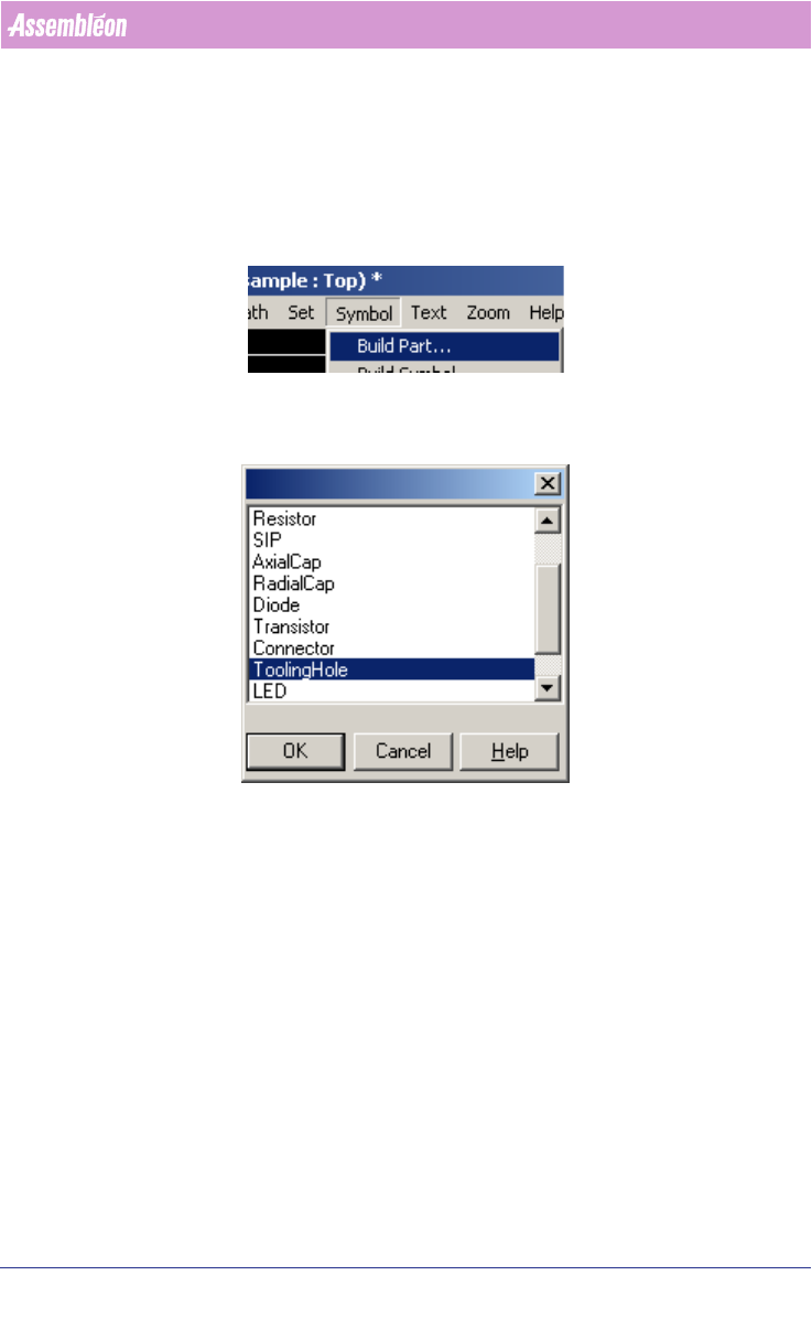
1. Take care that no other item is selected (use ctrl-d to ensure this) Click on
one circle in the MDF editor (it is not correct to select all circles since that
would turn them into one object). The circle is now the only purple object
shown.
2. Select Symbol > Build Part
3. Select ToolingHole from the selection list:
4. Click on the next circle and repeat step 3 until all (required) circles have
been turned into ToolingHoles.
2.14 Fiducial arrangements and Badmark Grouping
As the number of circuits on a PCB increases, the number of fiducial meas-
urements and (possible) badmark sensing activities performed by a Camera
also increases. In some cases the time that is needed by the Camera will
dominate the cycle time of the entire machine, which is not desirable. To
avoid this domination the concepts of fiducial arrangements
(see 2.15 on page
48) and badmark groupings (PowerLine) (see 2.16 on page 48) or area
badmarks can be used.
Fiducial arrangements enable the usage of the same set of fiducials for
multiple circuits.
User Manual 4022 591 98247
48 PPS-Pro v8.2 05.07
PPS-Pro GUI
2.15 Fiducial arrangement
A fiducial arrangement is an arbitrary set of fiducials plus an arbitrary set of
boards (=circuits) grouped together.
The purpose of the fiducial arrangement is to use the same fiducials for the
alignment of several boards (circuits). The result is a reduced number of
fiducials, which reduces the time required for fiducial measurements.
The creation of fiducial arrangement groups is performed using the MDF editor
(see 2.17 on page 50). One fiducial set per arrangement group can be defined
by the user. A maximum of 64 (on FCMs in extended mode 512) arrangements
per PCB can be defined.
2.16 BadMark Group
A badmark group (Reject Group) is a single panel-level badmark plus an
arbitrary set of board instances grouped together.
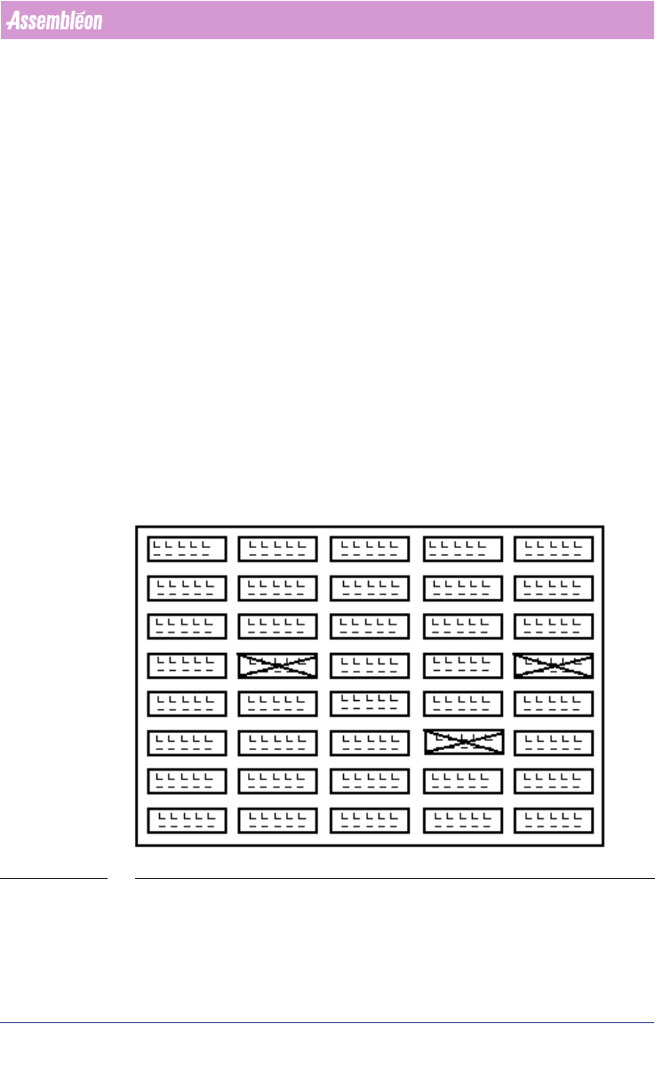
A number of applications are characterized by the fact that their PCBs have
many identical boards (=circuits).
Often there are tens to hundreds of identical boards per PCB (see FIGURE 4 on
page 48).
FIGURE 4 Circuit Badmarks
In many cases the circuit patterns on the PCB are tested in an earlier phase
and some of them are marked “bad” in this phase. This means the Machine
should not mount components on these boards (indicated by the crosses).

4022 591 98247 User Manual
05.07 PPS-Pro v8.2 49
PPS-Pro GUI
Each “bad” board (circuit) contains a circuit badmark (see FIGURE 4 on page
48). Badmarks are detected by a camera.
This camera will perform (in this example) 144 badmark measurements (1 per
circuit) In doing so, the processing time increases the pick-and-place time of
the placement modules. To decrease this influence, the processing time can be
reduced by introducing master badmarks. (And/or area badmarks on A-Series
lines)
Each badmark group has one master badmark. To maintain downward compat-
ibility, the pcb master badmark can also be used.
Two common types of badmarks exist:
1. Panel badmark;
2. Board (circuit) badmark;
In grouping mode multiple panel badmarks can be used. (see 2.19 "Set
Badmark Grouping" on page 56)
For A-Series users it is also possible to specify Area badmarks. (see 2.20 "Area
Badmarks (A-Series)" on page 57)
If more than one badmark type is used and one circuit is bad, the next ‘lower’
level type of badmark has to be provided.
Example: the badmark corresponding to the circuit, the master badmark of
the badmark group (FCM) or Area badmark (A-Series) to which the circuit
belongs, and the PCB master badmark.
For PowerLine users it is important to know that, if all three badmark levels
are available in the PCB description, the generated action specification will
not contain the PCB master badmark, only the circuit badmark and the group
master badmarks will be propagated to the Machine action specification or
Placement Program.
2.16.1 Panel Badmark
A panel badmark corresponds to a group of boards (circuits), each with its
own circuit badmark. If circuit badmarks are also present then panel
badmark(s) will become master badmark(s), they can be interpreted as a
“search” mark indicating that a search for circuit badmarks is necessary
(see
FIGURE 5 on page 50). A panel badmark may appear anywhere on the PCB.
Typically, master badmarks can be placed along a border of the PCB to reduce
travel time between master badmarks.
The figure 5 shows the PCB with 3 panel badmarks indicating a bad circuit in
their respective badmark groups.