00191017-01.pdf - 第529页
User ’s Manual Line Computer UNIX 17.3 Description of Components and P CBs Software V ersion 403.xx Edition 06/97 17.3.2 PCB 2: Focus on Package F orm Description 17 - 3 1 To create the first pin group (pins 5 and 7) at …
17.3 Description of Components and PCBs User’s Manual Line Computer UNIX
17.3.2 PCB 2: Focus on Package Form Description Software Version 403.xx Edition 06/97
17 - 30
continued from page 17-28
Entering handling
data
Package form description for package form 1503
Creating pin group
Accepting pin model
Creating pin group
Defining pin model
continued on page 17-32
User’s Manual Line Computer UNIX 17.3 Description of Components and PCBs
Software Version 403.xx Edition 06/97 17.3.2 PCB 2: Focus on Package Form Description
17 - 31
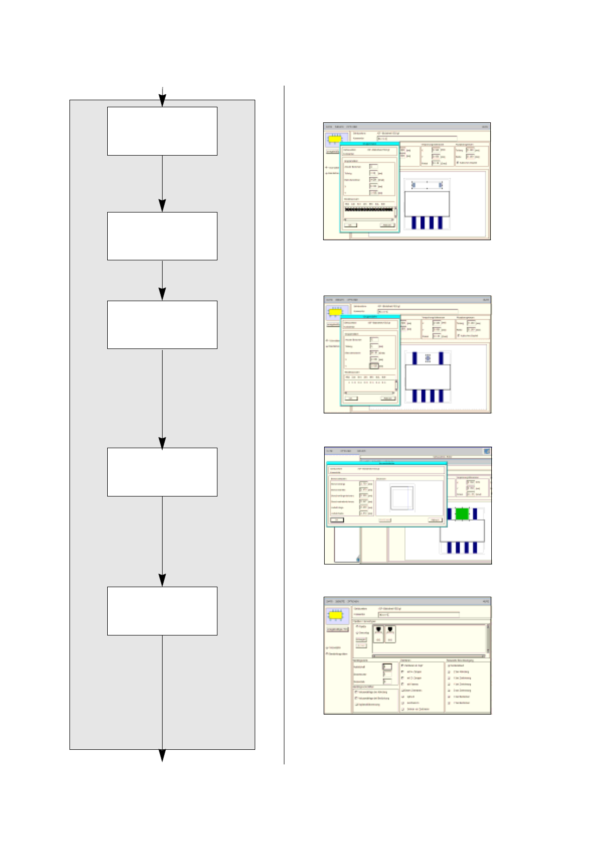
To create the first pin group (pins 5 and 7) at the top and to adopt the pin model from the pin group at
the bottom, proceed as follows:
75. Click on the
Create
button.
The Group data window is opened.
76. Overwrite the default values in the editing fields with the pin group data for package form 1503 (see dis-
plays in On-Line Help) and confirm by pressing the Enter key, here: see chart:
Every time the Enter key is pressed, the display of the pin group (gray areas) is updated.
77. In the selection field Model selection click on the model data of the lower pin group created.
78. Click on the
OK
button.
The Group data window is closed. The Model data for the upper pin group are adopted. The package
form is now displayed with the pins on the bottom side and the two pins on the top side.
To create the second pin group at the top (pin 6), proceed as follows:
79. Click on the
Create
button.
The Group data window is opened.
80. Overwrite the default values in the editing fields with the Pin group data for package form 1503 (see dis-
plays in On-Line Help) and confirm the entry by pressing the Enter key, here: see chart:
Every time the Enter key is pressed the display of the pin group (gray areas) is updated.
81. Click on the
OK
button.
The Group data window is closed.
To define the pin model for the second pin group at the top, proceed as follows:
82. Select one of the two pin groups by clicking on it.
83. Click on the
Pin/Ball
button.
The Pin model data window is opened.
84. Enter the pin model data, here: see chart:
In this example, the automatically calculated values of the other editing fields can be adopted.
The pin model is displayed graphically and updated after every entry.
85. Click on the
OK
button.
The Pin model data window is closed. The pins of the package forms are now completely defined. The
display corresponds to the package form on the data sheet.
To define the handling data for package form 1503, proceed as follows:
86. Activate the
Handling data
button.
The selection areas are displayed for entering the handling data.
87. In the Nozzles/Sensor types selection field activate the
Nozzle
button.
88. Click on the
Create
button.
The Nozzle type selection window containing a list of the nozzle types is opened.
89. Click on a nozzle, here:
615
.
The selection window is closed, the nozzle is adopted.
90. Select all other nozzle required accordingly, here:
618.
91. Activate the
Sensor type
button.
92. Click on the
Create
button.
The Sensor type selection window containing a list of the sensor types is opened.
93. Click on the sensor type
,
here:
9
.
The selection window is closed, the sensor type is adopted.
No. of pins Spacing Pin angle
X (BG
Off
) Y (BG
Off
)
1 1 90 0 2.625
Pin length BL Pin width b1
1.75 1.87
No. of pins Spacing e1 Pin angle
X (BG
Off
) Y (BG
Off
)
2 3.81 90 0 2.625
17.3 Description of Components and PCBs User’s Manual Line Computer UNIX
17.3.2 PCB 2: Focus on Package Form Description Software Version 403.xx Edition 06/97
17 - 32
FILE
Save
FILE
Save
FILE
Quit
Allocating a package
form to a feeder
continued from page 17-30
Saving package form
to feeder allocation
Package form description for pack. form 1503
continued on page 17-34
Saving package form
data