00191017-01.pdf - 第534页
17.3 Description of Components and PCBs User ’s Manual Line Computer UNIX 17.3.2 PCB 2: Focus on Package Form Description Software V ersion 403.xx Edition 06/ 97 17 - 36 PCB de scription Defin ing fiduc ials contin ued f…
User’s Manual Line Computer UNIX 17.3 Description of Components and PCBs
Software Version 403.xx Edition 06/97 17.3.2 PCB 2: Focus on Package Form Description
17 - 35
17.2.2.2 Component Description
To open the Component Editor for a component, proceed as follows:
104.On the desktop click on the icon the the Component Editor .
The file selection window is opened.
105.Click on the
Selection
editing field.
106.Enter the name of the component, here:
Comp4.be
, click on the
OK
button.
The Component Editor is opened.
To enter the component data, proceed as follows:
107.Click on the
Comment
editing field, enter a comment that is a unique description of the component, here:
Chip 2220
.
108.Click on the
Package form
editing field, enter the package form number, here:
1501
.
109.In the Handling selection field activate the appropriate buttons, here:
Placing
.
110.In the CRDL selection area activate the appropriate buttons, here:
No check
.
111.Click on the
Save
option on the
FILE
menu.
The component data are saved.
112.Click on the
Quit
option on the
FILE
menu.
The Component Editor is closed.
113.Carry out the component description for the remaining components analogously, here:
Comp5.be
and
Comp6.be
.
17.2.2.3 Adhesive Pattern Description
For the new package forms an adhesive pattern is automatically adopted from the DM-Bibliothek.
17.2.2.4 PCB Description
To open the PCB Editor, proceed as follows:
114.On the desktop click on the icon of the PCB Editor .
The file selection window is opened.
115.Click on the
Selection
editing field.
116.Enter the name of the PCB
,
here:
Example_2.la
and click on the
OK
button.
A dialog box is opened.
117.Click on the
TYPE
editing field.
118.Enter a type designation, here:
board_1
and click on the
OK
button.
The PCB Editor is opened. The PCB is displayed as a rectangle.
To specify the position of the PCB in the machine, proceed as follows:
119.Activate the Coordinate system icon .
120.Click on the PCB (rectangle).
A dialog box with the display of four coordinate systems is opened.
121.Click on a coordinate system, here:
0°
.
122.Click on the
OK
button.
The dialog box is closed.
17.3 Description of Components and PCBs User’s Manual Line Computer UNIX
17.3.2 PCB 2: Focus on Package Form Description Software Version 403.xx Edition 06/97
17 - 36
PCB description
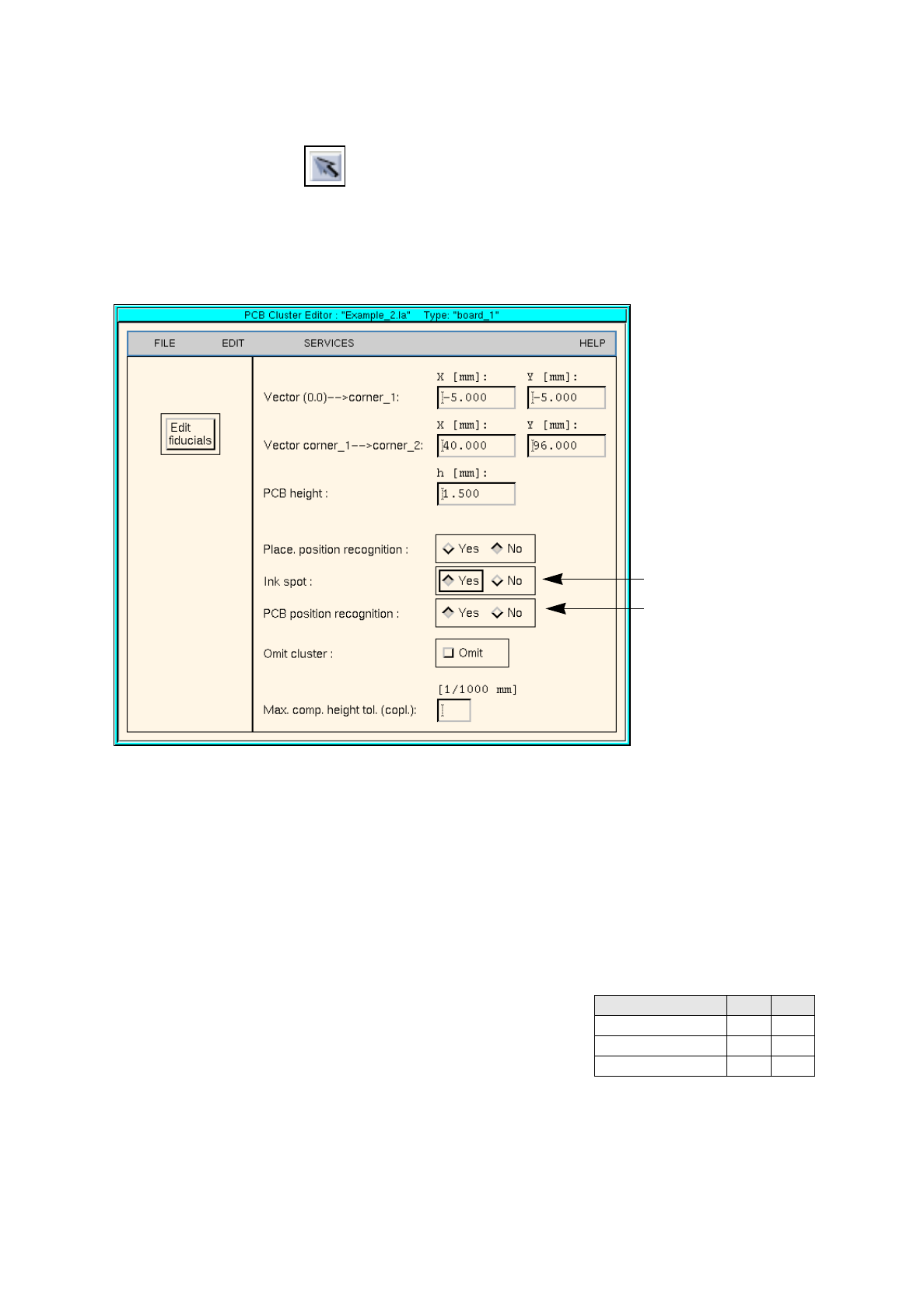
Defining fiducials
continued from page 17-34
Entering dimensions
of the PCB
continued on page 17-38
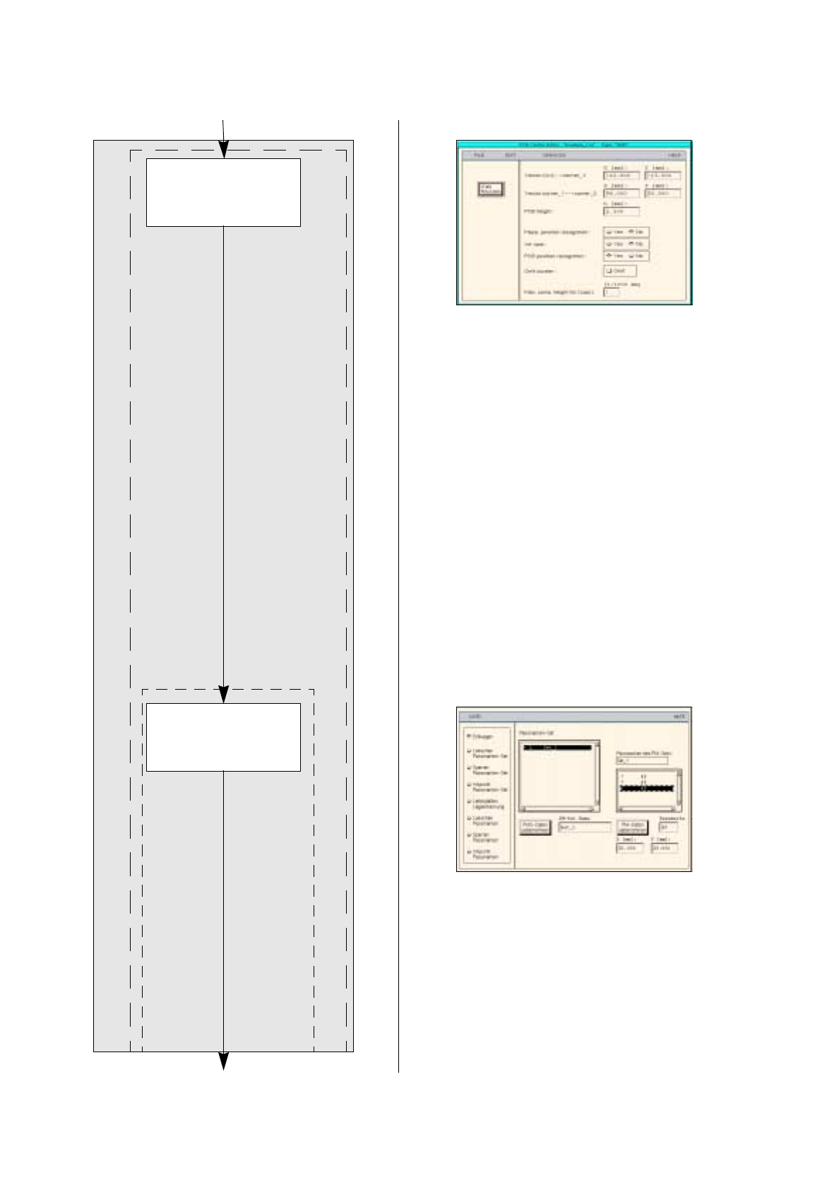
Cluster Editor
Fiducial Editor
User’s Manual Line Computer UNIX 17.3 Description of Components and PCBs
Software Version 403.xx Edition 06/97 17.3.2 PCB 2: Focus on Package Form Description
17 - 37
To enter the dimensional data of the PCB, proceed as follows:
123.Activate the Select icon .
124.Click on the PCB (rectangle).
The rectangle is highlighted in green.
125.Click on the
Cluster Editor
option on the
SERVICES
menu.
The Cluster Editor is opened.
126.Enter the dimensions of the PCB. See
Fig. 17.3.4
on page 17-
20
and
Fig. 17.3.5
.
Fig. 17.3.5 Cluster Editor for PCB 2
To define the fiducials, proceed as follows:
127.In the Cluster Editor click on the
Edit fiducials
button.
The Fiducial Editor is opened.
128.Activate the
Insert
button.
129.Click on the
Fiducial set name
editing field.
130.Enter a name for the new fiducial set, here:
Set_1
.
131.Click on the
Accept fiducial set
button.
The fiducial set Set_1
appears on the fiducial list.
132.Click on fiducial set Set_1 on the fiducial list.
133.Click on the
Fiducial
editing field.
134.Enter the fiducial number for the first fiducial, here:
48
.
135.Click on the editing fields for the coordinates, enter coordinates
(do not confirm with Enter key!), here: see chart:
136.Click on the
Accept fiducial data
button.
The data of the fiducial are transferred to the list of the fiducials of the fiducial set.
137.Define the remaining fiducials accordingly, here:
fiducials
48
and
48
.
138.Activate the
PCB position recognition
button.
139.Click on the fiducial set Set_1 on the fiducial list.
The fiducial set
Set_1
is marked by a preceeding
L
for PCB position recognition.
Fiducial number X Y
48 30 0
48 0 86
48 30 86
Activate ink spot
Activate PCB pos. recognition