00191017-01.pdf - 第541页
User ’s Manual Line Computer UNIX 17.3 Description of Components and P CBs Software V e rsion 403.xx Ed ition 06/97 17.3.3 PCB 3: Focus on C luster T echnique 17 - 4 3 17.2.3.1 Package form description PCB 3 consis ts of…
17.3 Description of Components and PCBs User’s Manual Line Computer UNIX
17.3.3 PCB 3: Focus on Cluster Technique Software Version 403.xx Edition 06/97
17 - 42
The package form description is dispensed with.
The component description is dispensed with.
The adhesive pattern description is dispensed with.
No fiducials are present.
No ink spot is present.
The placement positions are defined in the
single circuits.
Pack. form description
Starting the PCB
Editor for a PCB
Indicating position of
PCB in the machine
Defining ink spot
Component description
Adh. pattern description
Entering dimensions
of PCB
Defining fiducials
continued on page 17-44
Cluster Editor
Fiducial Editor
Entering placement
positions
PCB description
User’s Manual Line Computer UNIX 17.3 Description of Components and PCBs
Software Version 403.xx Edition 06/97 17.3.3 PCB 3: Focus on Cluster Technique
17 - 43
17.2.3.1 Package form description
PCB 3 consists of four clusters with three single circuits each, all of which correspond to PCB 2.
For the package form description refer to
section 17.2.2.1
17.2.3.2 Component description
PCB 3 consists of four clusters with three single circuits each, all of which correspond to PCB 2.
For the component description refer to
section 17.2.2.2
17.2.3.3 Adhesive pattern description
PCB 3 consists of four clusters with three single circuits each, all of which correspond to PCB 2.
For the adhesive pattern description refer to
section 17.2.2.3
.
17.2.3.4 PCB description
The offset values are to be determined automatically from
Fig. 17.3.7
on page 17-
41
(solution on page 17-
51
).
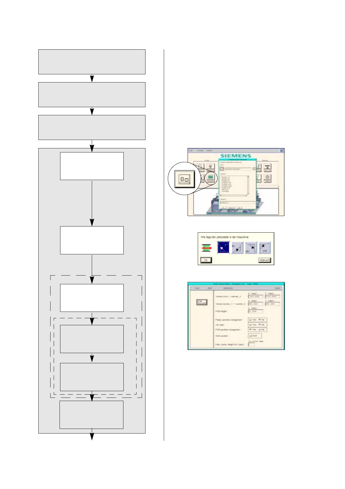
To open the PCB Editor for a PCB, proceed as follows:
1. On the desktop click on the icon the PCB Editor .
The file selection window is opened.
2. Click on the
Selection
editing field.
3. Enter the name of the PCB
,
here:
Example_3.la,
and click on the
OK
button.
A dialog box is opened.
4. Click on the
TYPE
editing field.
5. Enter a type designation, here:
Typ_1,
and click on the
OK
button:
The Component Editor is opened. The PCB is displayed as a rectangle.
To specify the position of the PCB in the machine:
6. Activate the Coordinate system icon .
7. Click on the PCB (rectangle).
A dialog box containing the display of four coordinate systems is opened.
8. Click on a coordinate system, here:
0°
.
9. Click on the
OK
button.
The dialog box is closed.
To enter the dimensions of the PCB, proceed as follows:
10. Activate the Select icon .
11. Click on the PCB (rectangle).
The rectangle is highlighted in green.
12. Click on the
Cluster Editor...
option on the
SERVICES
menu.
The Cluster Editor is opened.
13. Enter the dimensions of the PCB, see
Fig. 17.3.7
on page 17-
41
.
14. Click on the
Quit
option on the
FILE
menu.
The Cluster Editor is closed.
Defining fiducials:
no fiducials are present.
Defining ink spot:
no ink spot is present.
Entering placement positions:
the placement positions are defined at a later point in the single circuits.
17.3 Description of Components and PCBs User’s Manual Line Computer UNIX
17.3.3 PCB 3: Focus on Cluster Technique Software Version 403.xx Edition 06/97
17 - 44
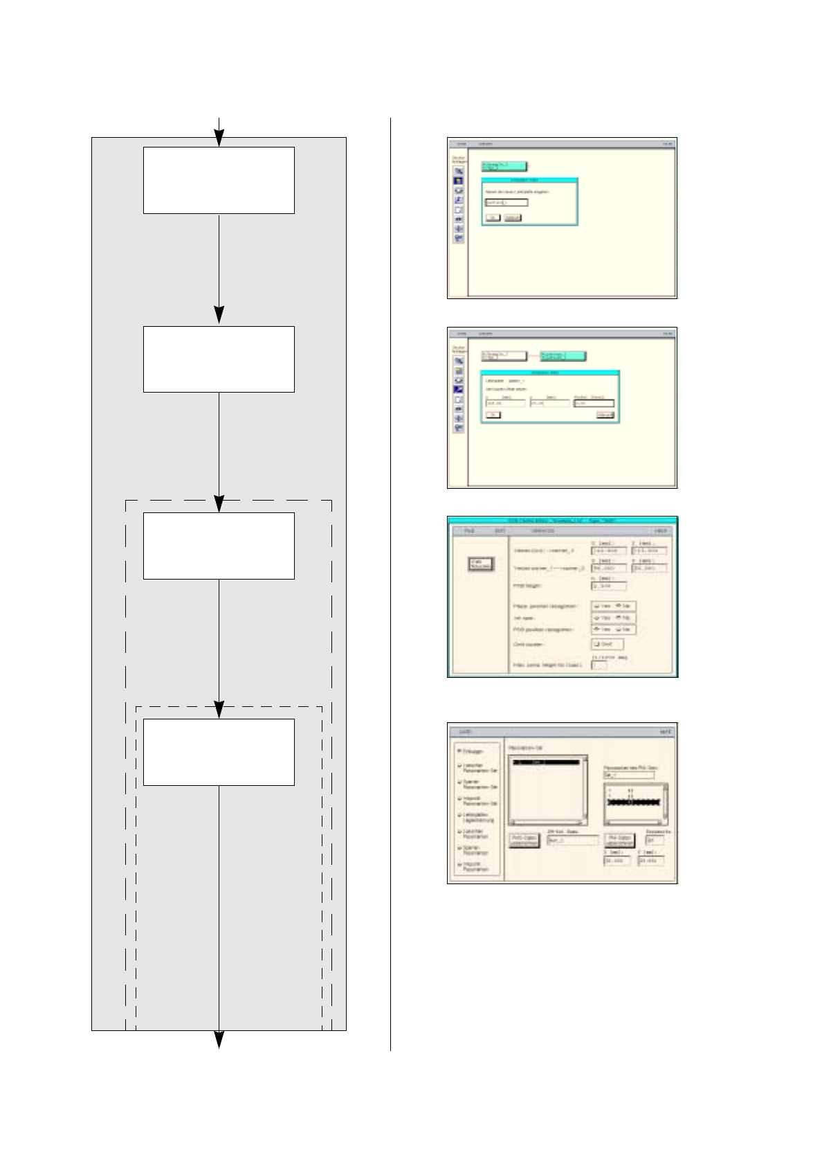
Creating a cluster
continued on page 17-46
continued from page 17-42
Entering offset values
for the cluster
Entering dimensions
of the cluster
Defining
fiducials
Cluster Editor
Fiducial Editor
PCB description