SIPLACE Line Computer UNIX.pdf - 第560页
17 Practical Tips on Using the LC UNIX User Manual Line Computer UNIX 17.3 Description of Com ponents and PC Bs Software Version 5 02.xx 10 /2000 Issue 558 I t I I No ink sp ot is present. Loading c luster data and plac …
User Manual Line Computer UNIX 17 Practical Tips on Using the LC UNIX
Software Version 502.xx 10/2000 Issue 17.3 Description of Components and PCBs
557
I
t I I
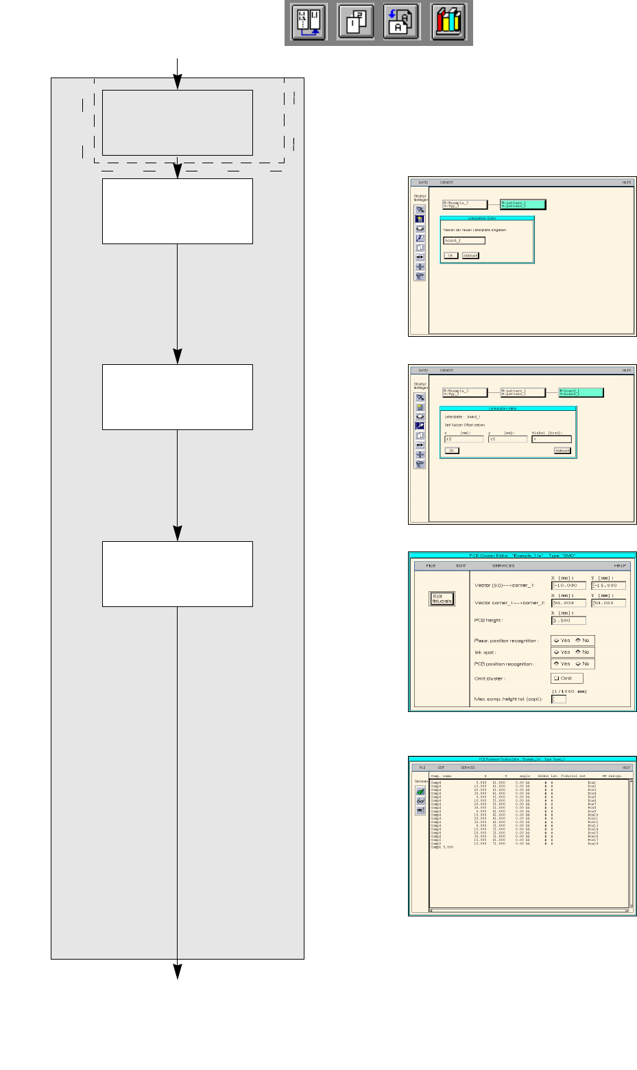
To create a cluster on the PCB, create as follows:
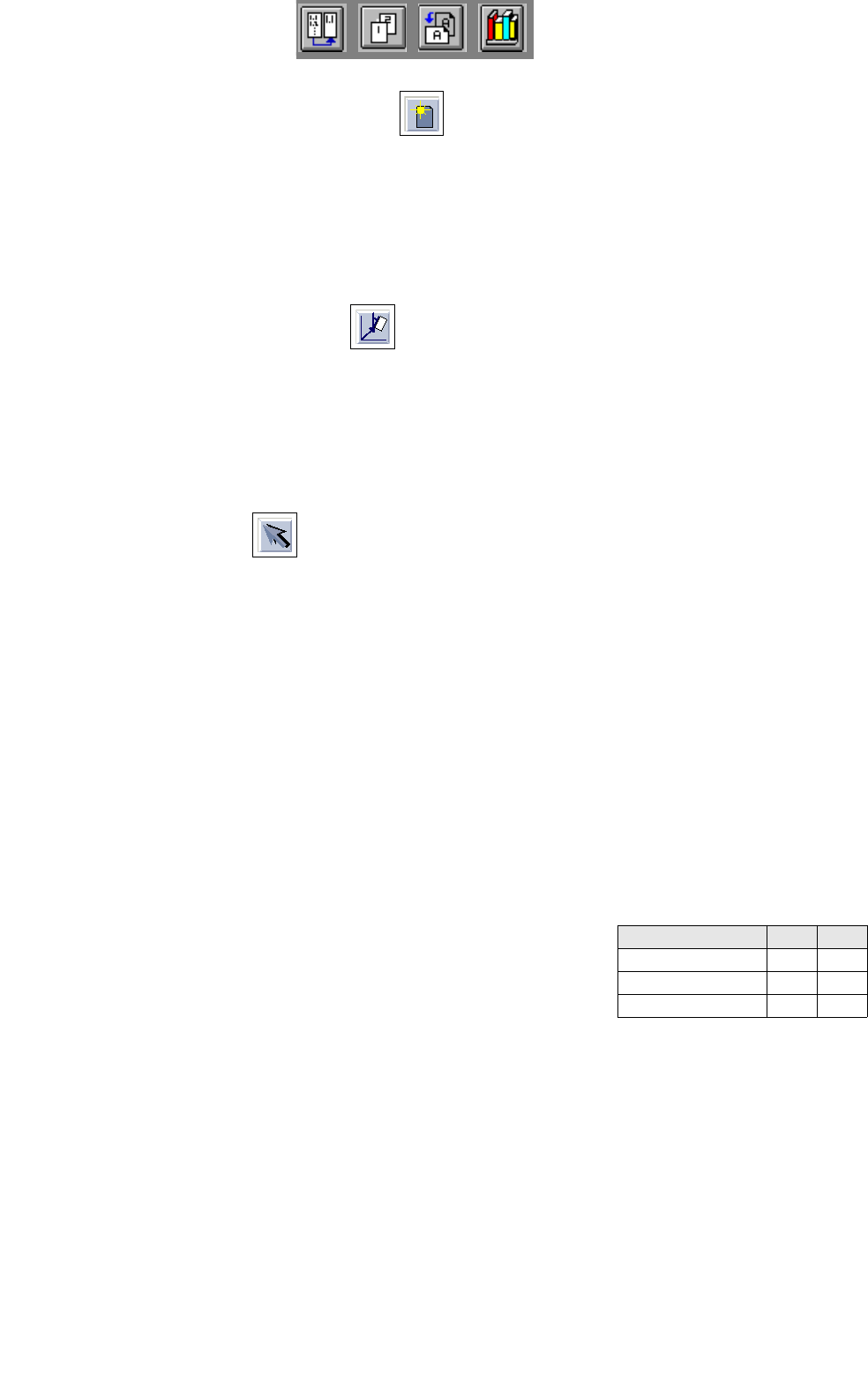
15. In the PCB Editor, activate the Create icon .
16. Click on the PCB, here: Example_3.
A dialog box is opened.
17. Click on the editing field.
18. Enter the name of the cluster, here: pattern_1, and click on the OK button.
The dialog box is closed. The new cluster is displayed at the second level.
To enter the cluster offset values, proceed as follows:
19. Activate the Coordinate system icon .
20. Click on the cluster, here: pattern_1.
A dialog box is opened.
21. Click on the individual editing fields and enter the offset values, see Fig. 17.3.7 on page 17-553.
22. Click on the OK button.
The dialog box is closed.
To enter the dimensions of the cluster, proceed as follows:
23. Activate the Select icon .
24. Click on the cluster, here: pattern_1.
25. Click on the Cluster Editor option on the SERVICES menu.
The Cluster Editor is opened.
26. Enter the dimensions of the cluster, see Fig. 17.3.7 on page 17-553.
To define the fiducials for the cluster, proceed as follows:
27. In the Cluster Editor click on the Edit fiducials button.
The Fiducial Editor is opened.
28. Activate the Insert button.
29. Click on the Fiducial set name editing field.
30. Enter a name for the new fiducial set, here: Set_1.
31. Click on the OK button.
The fiducial set Set_1 appears on the fiducial list.
32. Click on the fiducial set Set_1 on the fiducial list.
33. Click on the Fiducial editing field.
34. Enter the fiducial number for the first fiducial, here: 48.
35. Click on the individual editing fields for the coordinates, enter
coordinates do not confirm with the Enter key), here: see chart:
36. Click on the OK button.
The data of the fiducial are transferred to the list of the fiducials of the fiducial set.
37. Define the remaining fiducials analogously, here: fiducials 48 and 48.
38. Activate the PCB position recognition button.
39. Click on the fiducial set Set_1 on the fiducial list.
The fiducial set name Set_1 is preceded by an
L for the PCB position recognition.
40. Click on the Quit option on the FILE menu.
The Fiducial Editor is closed.
41. Click on the Quit option on the FILE menu.
The Cluster Editor is closed.
Ficucial number X Y
48 5 5
48 5 111
48 145 5
17 Practical Tips on Using the LC UNIX User Manual Line Computer UNIX
17.3 Description of Components and PCBs Software Version 502.xx 10/2000 Issue
558
I
t I I
No ink spot is present.
Loading cluster data
and placement
positions
continued from page 17-44
Creating a single
circuit
continued on page 17-48
Entering offset values
for the single circuit
PCB description
Defining ink spot

User Manual Line Computer UNIX 17 Practical Tips on Using the LC UNIX
Software Version 502.xx 10/2000 Issue 17.3 Description of Components and PCBs
559
I
t I I
Defining ink spot: no ink spot is present.
To create a single circuit in a cluster, proceed as follows:
42. Activate the Create icon .
43. Click on the cluster, here: pattern_1.
A dialog box is opened.
44. Click on the editing field.
45. Enter the name for the single circuit, here: board_1, and click on the OK button.
The dialog box is closed. The new single circuit is displayed at the third level.
To enter the offset values for the single circuit, proceed as follows:
46. Activate the Coordinate system icon .
47. Click on the single circuit, here: board_1.
A dialog box is opened.
48. Click on the individual editing fields and enter the offset values, see Fig. 17.3.7 on page 17-553.
49. Click on the OK button.
The dialog box is closed.
To load the cluster data and placement positions of another PCB for the single circuit:
50. Activate the Select icon .
51. Click on the single circuit, here: board_1.
52. Click on the Cluster Editor option on the SERVICES menu.
The Cluster Editor is opened.
53. Click on the Structure Editor option on the SERVICES menu.
A file selection window is opened.
54. Select a PCB by double-clicking, here: Example_2.la.
The PCB Editor for Example_2.la is opened.
55. Click on the PCB (rectangle), here: Example_2.
56. Using the key combination Alt+Tab change to the Cluster Editor of the single circuit, here: board_1.
57. Click on the Load cluster data from option on the EDIT menu.
A dialog box containing the name of the source cluster is displayed.
58. Click on the OK button.
The cluster data of the other PCB, here: Example_2, are transferred to the current single circuit, here:
board_1, the dialog box is closed. The Placement Position Editor is opened.
59. Using the key combination Alt+Tab change to the PCB Editor of the other PCB, here: Example_2.la.
60. Click on the PCB, here: Example_2.la.
61. Using the key combination Alt+Tab change to the Placement Position Editor of the single circuit, here:
board_1.
62. Click on the Load placement position from option on the EDIT menu.
A dialog box containing the name of the source cluster is displayed.
63. Click on the OK button.
The placement positions of the other PCB, here: Example_2, are transferred to the single circuit, here:
board_1, the dialog box is closed.
64. Click on the Quit option on the FILE menu.
The Placement Position Editor is closed.