IPC J-STD-003B.pdf - 第12页
T est C – Solder Float T est For plated-through holes, sur - face conductors and attachment lands, solder source side (see 4.2.3) T est D – W ave Solder T est For plated-through holes, surface conductors and attachment l…

Solderability Tests for Printed Boards
1 GENERAL
1.1 Scope
This standard prescribes test methods, defect
definitions and illustrations for assessing the solderability
of printed board surface conductors, attachment lands, and
plated-through holes. This standard is intended for use by
both vendor and user.
1.2 Purpose The solderability determination is made to
verify that the printed board fabrication processes and sub-
sequent storage have had no adverse effect on the solder-
ability of those portions of the printed board intended to be
soldered. This is determined by evaluation of the solder-
ability test specimen portion of a board or representative
test specimen which has been processed as part of the
panel of boards and subsequently removed for testing per
the method selected.
1.3 Objective The objective of the solderability test
methods described in this standard is to determine the abil-
ity of printed board surface conductors, attachment lands,
and plated-through holes to wet easily with solder and to
withstand the rigors of the printed board assembly pro-
cesses.
1.3.1 Shall or Should The word ‘‘shall’’ is used in the
text of this document wherever there is a requirement for
materials, preparation, process control or acceptance of a
soldered connection or a test method. The word ‘‘should’’
reflects recommendations and is used to reflect general
industry practices and procedures for guidance only.
1.3.2 Document Hierarchy In the event of conflict, the
following descending order of precedence applies:
1. Procurement as agreed between user and supplier.
2. Master drawing or master assembly drawing reflecting
the user’s detailed requirements.
3. When invoked by the customer or per contractual agree-
ment, this document, J-STD-003.
4. Other documents to extent specified by the customer.
1.4 Performance Classes Three general classes have
been established to reflect progressive increases in sophis-
tication, functional performance requirements and testing/
inspection frequency. It should be recognized that there
may be an overlap of equipment categories in different
classes. The user has the responsibility to specify in the
contract or purchase order the performance class required
for each product and shall indicate any exceptions to spe-
cific parameters, where appropriate.
Class 1 – General Electronic Products
Includes consumer products, some computer and computer
peripherals suitable for applications where cosmetic imper-
fections are not important and the major requirement is
function of the completed printed board.
Class 2 – Dedicated Service Electronic Products
Includes communications equipment, sophisticated busi-
ness machines, instruments where high performance and
extended life is required and for which uninterrupted ser-
vice is desired but not critical. Certain cosmetic imperfec-
tions are allowed.
Class 3 – High Performance Electronic Products
Includes the equipment and products where continued per-
formance or performance on demand is critical. Equipment
downtime cannot be tolerated and must function when
required such as in life support items or flight control sys-
tems. Printed boards in this class are suitable for applica-
tions where high levels of assurance are required and ser-
vice is essential.
1.5 Method Classification This standard describes test
methods by which both the surface conductors (and attach-
ment lands) and plated-through holes may be evaluated for
solderability. Test A, Test B, Test C, Test D and Test E for
tin/lead solder processes and Test A1, Test B1, Test C1,
Test D1 and Test E1 for lead-free solder processes, unless
otherwise agreed upon between vendor and user. Test A
and Test C for tin/lead solder processes, Test A1 and Test
C1 for lead-free solder processes are to be used as a default
solderability tests.
Provisions are made for this determination to be performed
at the time of manufacture, at the receipt of the boards by
the user, or just prior to assembly and soldering. User and
vendor shall agree to the appropriate method to be used
and their correlation.
Standard dwell times are defined in some of the methods
called out in this standard. Variations in board heat capac-
ity may necessitate the use of longer solder dwell times
(see 6.2). Any change in solder dwell shall be agreed upon
by user and vendor.
1.5.1 Visual Acceptance Criteria Tests
Tin Lead Solder Alloy
Test A – Edge Dip Test For surface conductors and
attachment lands only (see 4.2.1)
Test B – Rotary Dip Test For plated-through holes, sur-
face conductors and attachment lands, solder source side
(see 4.2.2)
March 2007 IPC J-STD-003B
1
Copyright Association Connecting Electronics Industries
Provided by IHS under license with IPC
Not for Resale
No reproduction or networking permitted without license from IHS
--`,,```,,,,````-`-`,,`,,`,`,,`---
//^:^^#^~^^"^~"^"^:$^~#:"#:$@:~^"$^:#*~^$^~:^#*^^:^^*\\
Test C – Solder Float Test For plated-through holes, sur-
face conductors and attachment lands, solder source side
(see 4.2.3)
Test D – Wave Solder Test For plated-through holes,
surface conductors and attachment lands, solder source side
(see 4.2.4)
Test E – Surface Mount Simulation Test For surface
conductors and attachment lands (see 4.2.5)
Lead Free Solder Alloy
Test A1 – Edge Dip Test For surface conductors and
attachment lands only (see 4.2.6)
Test B1 – Rotary Dip Test For plated-through holes,
surface conductors and attachment lands, solder source side
(see 4.2.7)
Test C1 – Solder Float Test For plated-through holes,
surface conductors and attachment lands, solder source side
(see 4.2.8)
Test D1 – Wave Solder Test For plated-through holes,
surface conductors and attachment lands, solder source side
(see 4.2.9)
Test E1 – Surface Mount Simulation Test For surface
conductors and attachment lands (see 4.2.10)
1.5.2 Force Measurement Criteria Tests
Tin Lead Solder Alloy
Test F – Wetting Balance Test For plated-through holes,
surface conductors and attachment lands (see 4.3.1)
Lead Free Solder Alloy
Test F1 – Wetting Balance Test For plated-through
holes, surface conductors and attachment lands (see 4.3.2)
Tests F and F1 shall not be used for acceptance/rejection
without user and vendor agreement. Please forward all test
data generated using these test methods, including type of
board tested (such as Type 2 or 12 layer, Type 3), dimen-
sions of test specimen tested, and any pretreatment, to:
IPC
Attn. J-STD-003 Staff Liaison
3000 Lakeside Drive, Suite 309S
Bannockburn, IL 60015
1.5.3 Test(s) Methodologies Under Committee Review
The J-STD-003 committee has undertaken, characterized,
and reviewed the use of the Sequential Electrochemical
Reduction Analysis (SERA® methodology for solderability
testing. The committee’s current position is that the
SERA® test method should reside within the IPC-TM-650
manual until additional solderability test information is
generated. Please forward all test data for committee
review to:
IPC
Attn. J-STD-003 Staff Liaison
3000 lakeside Drive, Suite 309S
Bannockburn, IL 60015
1.6 Test Method Selection For appropriate test selection
refer to 1.5 and Tables 1-1 and 1-2. The test selection
should consider the final soldering process so that the
results of the test will best represent that process.
1.7 Test Specimen Requirements The test specimen
shall be a representative test specimen, a portion of the
printed board being tested, or a whole board if within size
limits, such that an immersion depth defined in the indi-
vidual method is possible. The test specimen shall be rep-
resentative of the lot being tested. When this test specimen
is to be used as a criterion for material acceptance, the
number of test specimens shall be defined by agreement
between the user and vendor.
Test specimens that may be used for rigid board surface
solderability and plated-through hole solderability are
detailed in the paragraph sections under the individual test
methods. Similar test specimens may be used provided
they reflect the board circuitry, hole, and construction, and
have been processed in conjunction with the printed board
being evaluated.
Table 1-1 Test Method Selection
Test Method Applies to Surface Features Plated-Through Holes
Tests with Visual Assessment Criteria
A – Edge Dip Test
A1 – Edge Dip Test
X N/A
B – Rotary Dip Test
B1 – Rotary Dip Test
X (Solder Source Side Only) X
C – Solder Float Test
C1 – Solder Float Test
X (Solder Source Side Only) X
D – Wave Solder Test
D1 – Wave Solder Test
X (Solder Source Side Only) X
E – Surface Mount Simulation Test
E1 – Surface Mount Simulation Test
X N/A
Tests with Force Measurement Criteria
F – Wetting Balance Test
F1 – Wetting Balance Test
XX
IPC J-STD-003B March 2007
2
Copyright Association Connecting Electronics Industries
Provided by IHS under license with IPC
Not for Resale
No reproduction or networking permitted without license from IHS
--`,,```,,,,````-`-`,,`,,`,`,,`---
//^:^^#^~^^"^~"^"^:$^~#:"#:$@:~^"$^:#*~^$^~:^#*^^:^^*\\
Unless otherwise specified, the land associated with a
plated-through hole shall be considered part of the plated-
through hole if it is used for through-hole attachment. In
this case, only tests for hole solderability apply. If the land
is used for surface attachment of parts, then such lands
shall be tested for both hole and surface solderability.
1.8 Coating Durability The user shall specify to the ven-
dor, as part of the purchase or ordering agreement, the
required coating durability. The following are guidelines
for determining the needed level of coating durability (not
product performance classes). Conditioning and solderabil-
ity testing shall be performed per Table 1-2.
Category 1 – Minimum Coating Durability
Intended for boards which will be soldered within 30 days
from the time of manufacture and are likely to experience
minimum thermal exposures.
Category 2 – Average Coating Durability
Intended for boards likely to experience storage up to six
months from the time of manufacture and moderate ther-
mal or solder exposures.
Category 3 – Maximum Coating Durability
Intended for boards likely to experience long storage (over
six months) from the time of manufacture, severe thermal
or solder processing steps, etc. It should be recognized that
there may be a cost premium or delivery delay associated
with boards ordered to this durability level.
1.9 Limitation This standard shall not be construed as a
production soldering or tinning procedure for preparing or
soldering of printed boards or assemblies.
2 APPLICABLE DOCUMENTS
The following documents of the issue currently in effect
form a part of this standard to the extent specified herein.
2.1 Industry
2.1.1 IPC
1
IPC-T-50 Terms and Definitions
IPC-TM-650 Test Methods Manual
J-STD-005 Requirements for Soldering Pastes
J-STD-006 Requirements for Electronic Grade Solder
Alloys and Fluxed and Non-Fluxed Solid Solders for Elec-
tronic Soldering Applications
3 REQUIREMENTS
3.1 Terms and Definitions
The definition of terms shall
be in accordance with IPC-T-50. Terms that have been
repeated from IPC-T-50 for convenience are indicated by
an asterisk (*).
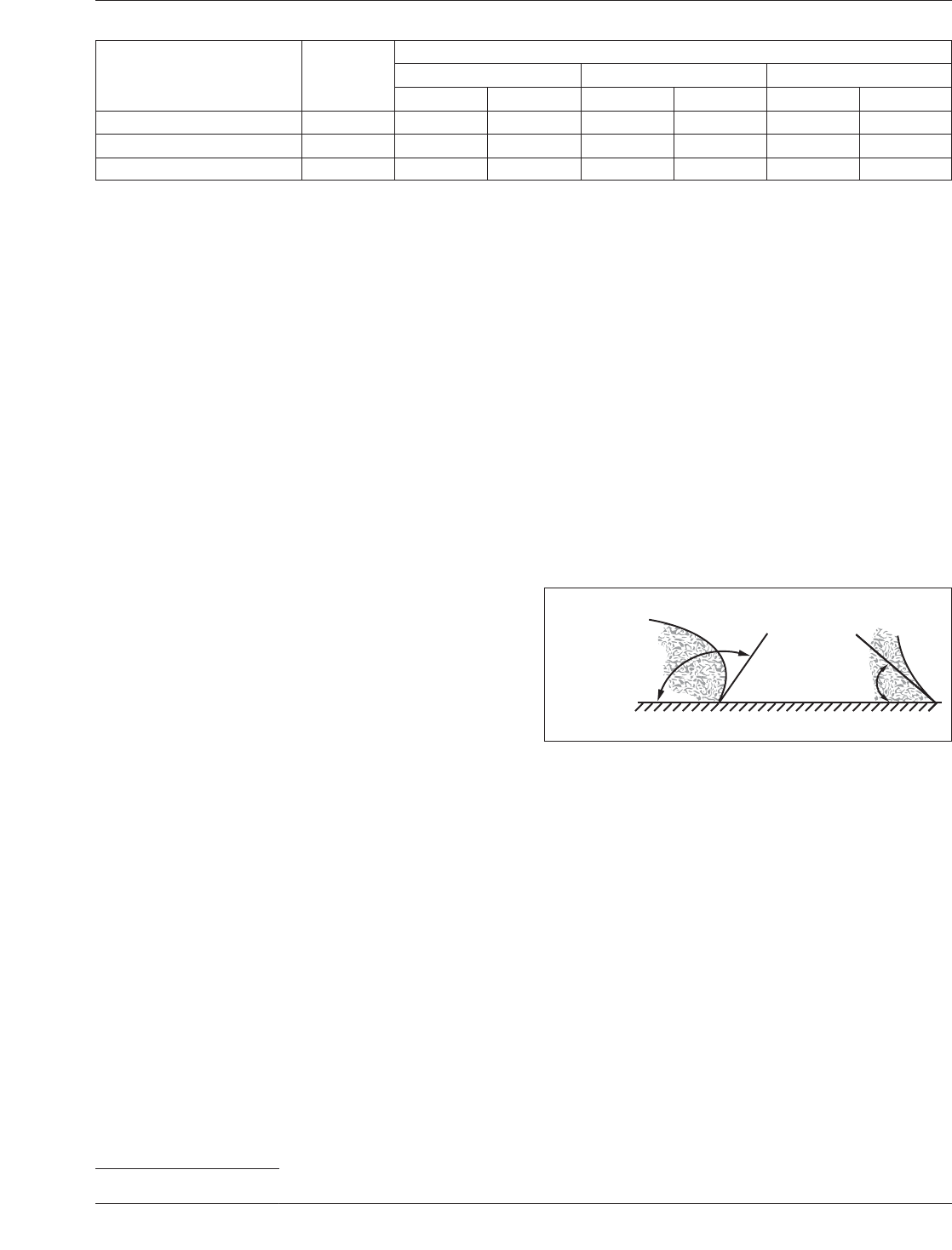
*Contact Angle, Soldering The angle of a solder fillet
that is enclosed between a plane that is tangent to the
solder/ basis-metal surface and a plane that is tangent to the
solder/ air interface (see Figure 3-1).
3.2 Materials
3.2.1 Solder
For tin/lead testing, the solder composition
shall be Sn60/Pb40, Sn62/Pb36/2Ag or Sn63/Pb37 per
J-STD-006. The composition of the solder, including con-
tamination levels, shall be maintained during testing per
3.5.2
The composition of the tin/lead solder paste to be used in
Test E shall be Sn60/Pb40 or Sn63/Pb37 for Sn/Pb per
J-STD-005, mesh size of -325/+500, flux type ROL1. The
solder paste shall meet the storage and shelf life require-
ments of the manufacturer’s specification.
For lead-free testing, the solder composition shall be
Sn96.5Ag3.0Cu0.5 (SAC305) per J-STD-006. Other lead-
free solder alloys may be used upon agreement between
user and vendor.
1. www.ipc.org
Table 1-2 Conditioning and Test Requirements
Pretest Conditioning Flux
Durability of Coating Rating
a
12
b
3
Surface Holes Surface Holes Surface Holes
8 Hours Conditioning (3.4.2) See 3.2.2 X
None See 3.2.2 X X X X
None Type
c
X
a. See 1.8.
b. Default Coating Rating.
c. Flux product used in the printed assembly process.
SOLDER
SMALL CONTACT
ANGLE
LARGE CONTACT
ANGLE
IPC-003b-3-1
Figure 3-1 Contact Angle
March 2007 IPC J-STD-003B
3
Copyright Association Connecting Electronics Industries
Provided by IHS under license with IPC
Not for Resale
No reproduction or networking permitted without license from IHS
--`,,```,,,,````-`-`,,`,,`,`,,`---
//^:^^#^~^^"^~"^"^:$^~#:"#:$@:~^"$^:#*~^$^~:^#*^^:^^*\\