IPC J-STD-003B.pdf - 第14页
The composition of the lead-free solder paste to be used in T est S1 shall be Sn96.5Ag3.0Cu0.5 (SAC305) per J-STD- 005, mesh size of -325/+500, flux type to be agreed upon between user and vendor . The solder paste shall …
Unless otherwise specified, the land associated with a
plated-through hole shall be considered part of the plated-
through hole if it is used for through-hole attachment. In
this case, only tests for hole solderability apply. If the land
is used for surface attachment of parts, then such lands
shall be tested for both hole and surface solderability.
1.8 Coating Durability The user shall specify to the ven-
dor, as part of the purchase or ordering agreement, the
required coating durability. The following are guidelines
for determining the needed level of coating durability (not
product performance classes). Conditioning and solderabil-
ity testing shall be performed per Table 1-2.
Category 1 – Minimum Coating Durability
Intended for boards which will be soldered within 30 days
from the time of manufacture and are likely to experience
minimum thermal exposures.
Category 2 – Average Coating Durability
Intended for boards likely to experience storage up to six
months from the time of manufacture and moderate ther-
mal or solder exposures.
Category 3 – Maximum Coating Durability
Intended for boards likely to experience long storage (over
six months) from the time of manufacture, severe thermal
or solder processing steps, etc. It should be recognized that
there may be a cost premium or delivery delay associated
with boards ordered to this durability level.
1.9 Limitation This standard shall not be construed as a
production soldering or tinning procedure for preparing or
soldering of printed boards or assemblies.
2 APPLICABLE DOCUMENTS
The following documents of the issue currently in effect
form a part of this standard to the extent specified herein.
2.1 Industry
2.1.1 IPC
1
IPC-T-50 Terms and Definitions
IPC-TM-650 Test Methods Manual
J-STD-005 Requirements for Soldering Pastes
J-STD-006 Requirements for Electronic Grade Solder
Alloys and Fluxed and Non-Fluxed Solid Solders for Elec-
tronic Soldering Applications
3 REQUIREMENTS
3.1 Terms and Definitions
The definition of terms shall
be in accordance with IPC-T-50. Terms that have been
repeated from IPC-T-50 for convenience are indicated by
an asterisk (*).
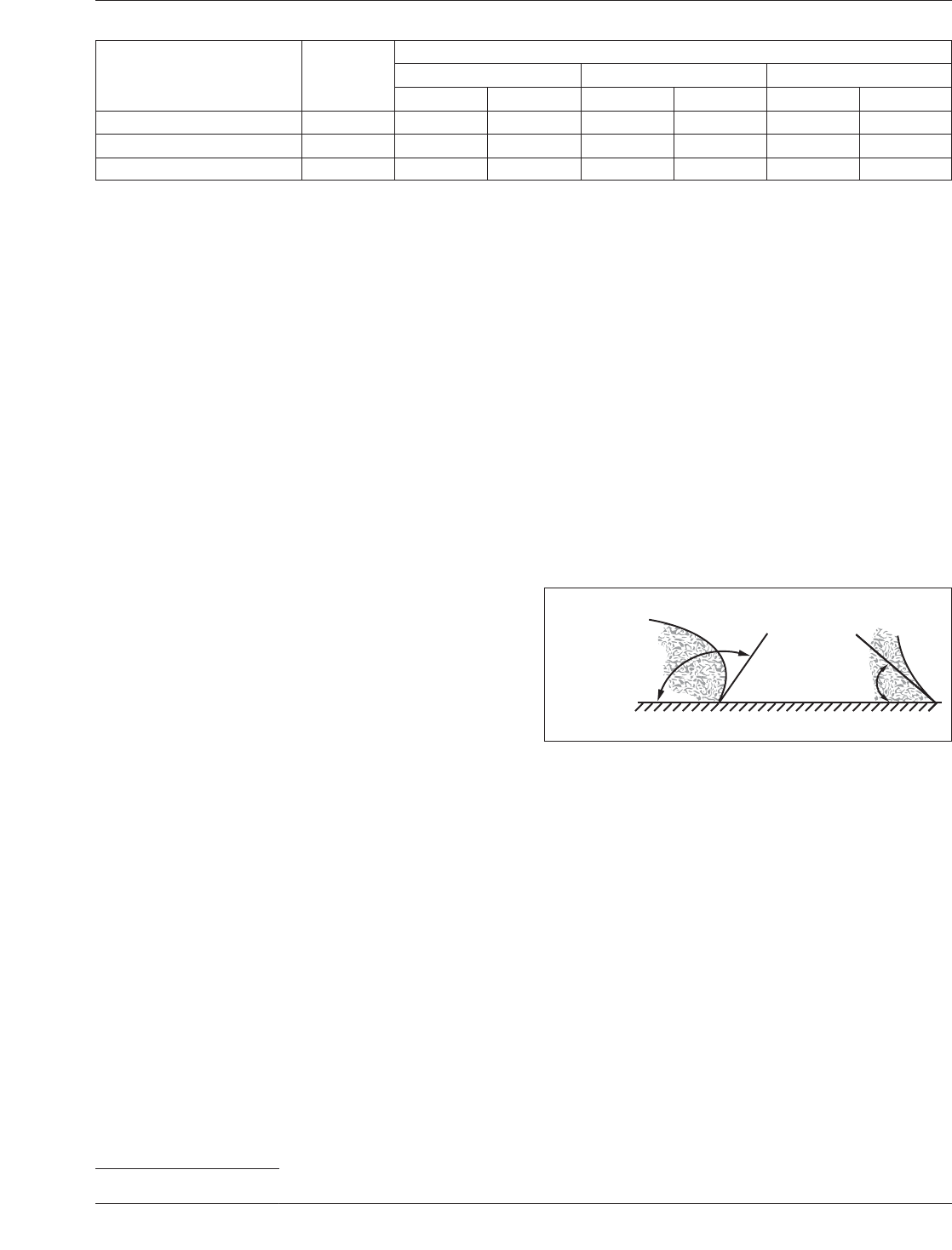
*Contact Angle, Soldering The angle of a solder fillet
that is enclosed between a plane that is tangent to the
solder/ basis-metal surface and a plane that is tangent to the
solder/ air interface (see Figure 3-1).
3.2 Materials
3.2.1 Solder
For tin/lead testing, the solder composition
shall be Sn60/Pb40, Sn62/Pb36/2Ag or Sn63/Pb37 per
J-STD-006. The composition of the solder, including con-
tamination levels, shall be maintained during testing per
3.5.2
The composition of the tin/lead solder paste to be used in
Test E shall be Sn60/Pb40 or Sn63/Pb37 for Sn/Pb per
J-STD-005, mesh size of -325/+500, flux type ROL1. The
solder paste shall meet the storage and shelf life require-
ments of the manufacturer’s specification.
For lead-free testing, the solder composition shall be
Sn96.5Ag3.0Cu0.5 (SAC305) per J-STD-006. Other lead-
free solder alloys may be used upon agreement between
user and vendor.
1. www.ipc.org
Table 1-2 Conditioning and Test Requirements
Pretest Conditioning Flux
Durability of Coating Rating
a
12
b
3
Surface Holes Surface Holes Surface Holes
8 Hours Conditioning (3.4.2) See 3.2.2 X
None See 3.2.2 X X X X
None Type
c
X
a. See 1.8.
b. Default Coating Rating.
c. Flux product used in the printed assembly process.
SOLDER
SMALL CONTACT
ANGLE
LARGE CONTACT
ANGLE
IPC-003b-3-1
Figure 3-1 Contact Angle
March 2007 IPC J-STD-003B
3
Copyright Association Connecting Electronics Industries
Provided by IHS under license with IPC
Not for Resale
No reproduction or networking permitted without license from IHS
--`,,```,,,,````-`-`,,`,,`,`,,`---
//^:^^#^~^^"^~"^"^:$^~#:"#:$@:~^"$^:#*~^$^~:^#*^^:^^*\\
The composition of the lead-free solder paste to be used in
Test S1 shall be Sn96.5Ag3.0Cu0.5 (SAC305) per J-STD-
005, mesh size of -325/+500, flux type to be agreed upon
between user and vendor. The solder paste shall meet the
storage and shelf life requirements of the manufacturers’
specification. Other lead-free solder pastes may be used
upon agreement between user and vendor
3.2.2 Flux The flux for tin/lead solderability tests shall
be a standard activated rosin flux #1 having a composition
of 25% ± 0.5% by weight of colophony and 0.15% ±
0.01% by weight diethylammonium hydrochloride (CAS
660-68-4), in 74.85% ± 0.5% by weight of isopropyl alco-
hol (see Table 3-1).
The flux for lead-free solderability tests shall be standard
activated rosin flux #2 having a composition of 25% ±
0.5% by weight of colophony and 0.39% ± 0.01% by
weight diethylammonium hydrochloride (CAS 660-68-4),
in 74.61% ± 0.5% by weight of isopropyl alcohol (see
Table 3-1).
3.2.2.1 Flux Maintenance Standard activated rosin
fluxes #1 and #2 shall be covered when not in use and dis-
carded after eight hours or the flux shall be maintained to
a specific gravity of 0.843 ± 0.005 at 25±2°C[77±3.6
°F] and discarded after one week of use.
3.2.3 Flux Removal Material used for cleaning printed
boards after solderability testing and prior to solderability
evaluations shall be capable of removing visible flux resi-
dues.
3.3 Equipment The following criteria applies to all
methods and equipment (see APPENDIX C for a list of
equipment sources). Equipment that is specific to any of
the solderability test methods is described within the
method details.
3.3.1 Conditioning Equipment The conditioning equip-
ment shall be capable of maintaining the temperature and
humidity parameters specified in 3.4.2. The test specimens
shall be suspended so that no portion of the test specimen
is within 40 mm [1.57 in] of the test chamber walls. The
nonmetallic holders shall support the test specimens
between vertical to 45 ° angle during exposure. Care shall
be taken to not exceed the capacity of the conditioning
equipment. Excessive or improper loading will cause con-
densation of humidity on the surface of the test specimens.
3.3.2 Solder Pot/Bath A thermostatically controlled
static solder bath shall be used of adequate dimensions to
accommodate the test specimens. The solder bath shall
contain enough solder to maintain the temperature during
testing within the specified temperature limits (3.5.1) and
to prevent exceeding the contamination levels (3.5.2). The
wave solder pot temperature limits utilized for Test Method
D or Test Method D1 shall be defined by agreement
between the user and vendor. Precautions should be taken
to avoid solder pot/bath damage due to metal erosion when
using Lead-free solder alloys.
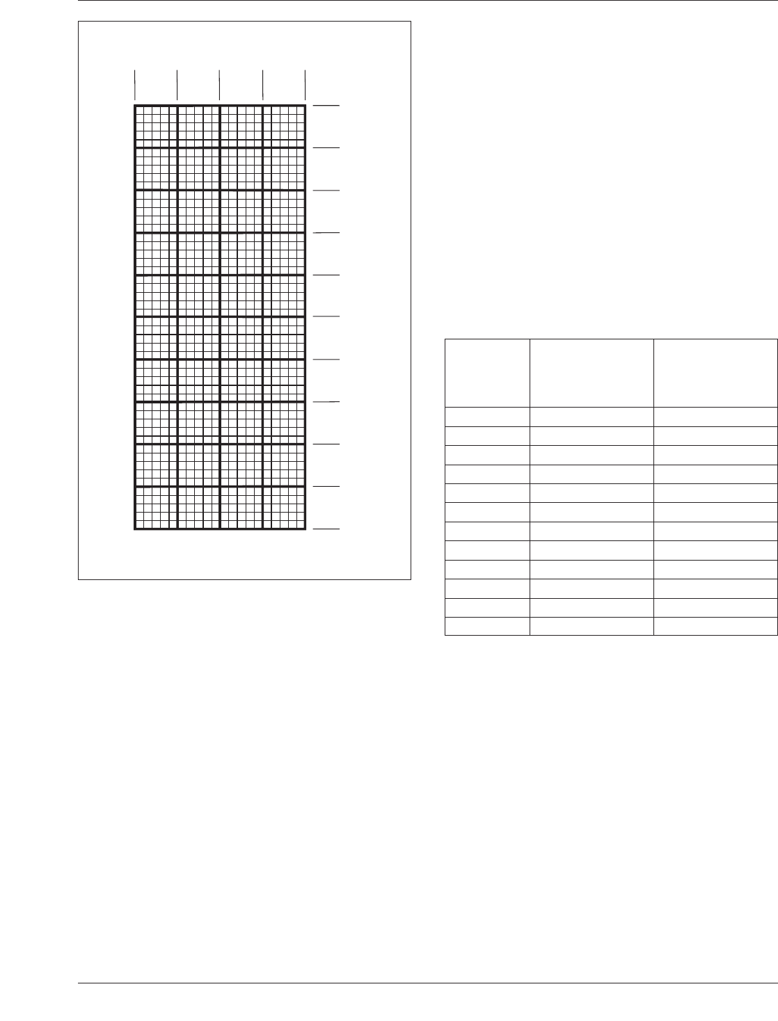
3.3.3 Optical Inspection Equipment All test methods
requiring visual inspection shall be capable of 10X magni-
fication (see individual test methods), and may be equipped
with reticles, or equivalent, for measurement, when appli-
cable. An example of a reticle is shown in Figure 3-2.
Shadowless lighting shall be used for proper inspection.
3.3.4 Dipping Equipment Solder dipping devices shall
be mechanical/electromechanical and capable of control-
ling the immersion/emersion rates dwell time and immer-
sion depth as specified in 4.2 to 4.3.
3.3.5 Timing Equipment Timing equipment shall be
automated and accurate to the limits of the test method.
3.4 Preparation for Testing
3.4.1 Test Specimen Preparation and Conditioning for
Test
Care shall be exercised to prevent contamination
(by grease, perspiration, etc.) of the surface to be tested.
When agreed upon between user and vendor, the test speci-
men to be tested may undergo other types of pretreatments
such as degreasing, aqueous cleaning, copper and solder
brightening, or baking.
The prescribed pretreatments should reproduce actual pro-
cessing of the printed boards up to the time of assembly
soldering (see 6.3). If conditioning is performed, prebaking
is not recommended.
3.4.2 Durability Conditioning All test specimens identi-
fied as requiring durability conditioning shall be subjected
to conditioning prior to solderability testing immediately
followed by a bake per 3.4.3. The durability test conditions
shall be 72 °C± 5 °C [162 °F ± 9 °F] and 85%± 3% Rela-
tive Humidity [RH]. The test specimens shall be exposed
for a test duration of eight hours ± 15 minutes.
3.4.3 Baking Immediately after conditioning and prior to
solderability testing, all boards shall be baked at 105 ± 5
°C [221 ± 9 °F] for 1 +1/-0 hours to remove surface mois-
ture and other volatiles. Test specimens shall be cooled to
room temperature prior to fluxing and testing.
Table 3-1 Flux Composition
Constituent
Composition by
Weight Percent
Flux #1 Flux #2
Colophony 25 ± 0.5 25 ± 0.5
Diethylammonium hydrochloride 0.15 ± 0.01 0.39 ± 0.01
Isopropyl Alcohol (IPA) Balance Balance
Weight of Chlorine as % of solids 0.2 0.5
Note: APPENDIX C: Informative Annex contains a listing of industry test
flux product sources.
IPC J-STD-003B March 2007
4
Copyright Association Connecting Electronics Industries
Provided by IHS under license with IPC
Not for Resale
No reproduction or networking permitted without license from IHS
--`,,```,,,,````-`-`,,`,,`,`,,`---
//^:^^#^~^^"^~"^"^:$^~#:"#:$@:~^"$^:#*~^$^~:^#*^^:^^*\\
3.5 Solder Bath Requirements
3.5.1 Solder Temperatures
Tin/lead solderability testing
shall be done at a solder temperature of 235±5°C[473 ±
9 °F]. Lead-free solderability testing shall be done at a sol-
der temperature of 255±5°C[491 ± 9 °F].
3.5.2 Solder Contamination Control The solder in
solder baths used for solderability testing shall be chemi-
cally or spectrographically analyzed or replaced each 30
operating days. The levels of contamination and Sn content
must be within those shown in Table 3-2. The intervals
between analysis may be lengthened if the test results indi-
cate that the contamination limits are not being
approached. The composition of the lead-free solder,
including contamination levels, shall be maintained during
testing per Table 3-2 with the silver and copper element
levels adjusted for alloy requirements.
NOTE: An operating day consists of any eight-hour
period, or any portion thereof, during which the solder is
liquefied and used.
If contamination exceeds the limits specified in Table 3-2,
then the solder shall be changed and the intervals between
analyses shall be shortened. A sampling plan shall be
developed, implemented, and documented, demonstrating
solder contamination process control.
20 15 10 5 0
0
5
1
0
15
2
0
25
3
0
35
4
0
45
5
0
IPC-003b-3-2
Figure 3-2 Example Reticle
Table 3-2 Maximum Limits of Solder Bath Contaminant
Contaminant
Maximum
Contaminant Weight
Percentage Limit
Sn Pb Alloys
a, b
Maximum
Contamination
Weight
Percentage Limit
Pb Free Alloys
a,c
Copper 0.300 0.800
Gold 0.200 0.200
Cadmium 0.005 0.005
Zinc 0.005 0.005
Aluminum 0.006 0.006
Antimony 0.500 0.500
Iron 0.020 0.020
Arsenic 0.030 0.030
Bismuth 0.250 0.250
Silver 0.100 4.000
Nickel 0.010 0.010
Lead N/A 0.100
Notes:
a. The tin content of the solder shall be maintained within ± 1% of the
nominal alloy being used. Tin content shall be tested at the same
frequency as testing for copper/gold contamination. The balance of the
bath shall be lead and/or the items listed above.
b. The total of copper, gold, cadmium, zinc, and aluminum contaminants
shall not exceed 0.4%. Not applicable to lead-free alloys.
c. These Maximum Contamination Weight Percentage Limits apply for
solderability testing using the SAC305 solder alloy. The use of other
lead-free solder alloys/maximum contamination weight percentage limits
may be used upon agreement between user and vendor.
March 2007 IPC J-STD-003B
5
Copyright Association Connecting Electronics Industries
Provided by IHS under license with IPC
Not for Resale
No reproduction or networking permitted without license from IHS
--`,,```,,,,````-`-`,,`,,`,`,,`---
//^:^^#^~^^"^~"^"^:$^~#:"#:$@:~^"$^:#*~^$^~:^#*^^:^^*\\